Optical modulation circuit and optical transmission system

Active Publication Date: 2010-09-02
NIPPON TELEGRAPH & TELEPHONE CORP
View PDF6 Cites 27 Cited by
  • Summary
  • Abstract
  • Description
  • Claims
  • Application Information

AI Technical Summary

Benefits of technology

[0030]According to the present invention, it is possible to implement multicarrier transmission capable of reducing the number of oscillators and the drive frequency that are required in generation of optica

Problems solved by technology

This leads to a problem of suppressing a nonlinear optical effect produced in the fiber such as self phase modulation (SPM

Method used


Image

  • Optical modulation circuit and optical transmission system
  • Optical modulation circuit and optical transmission system
  • Optical modulation circuit and optical transmission system

Examples


Example

First Embodiment

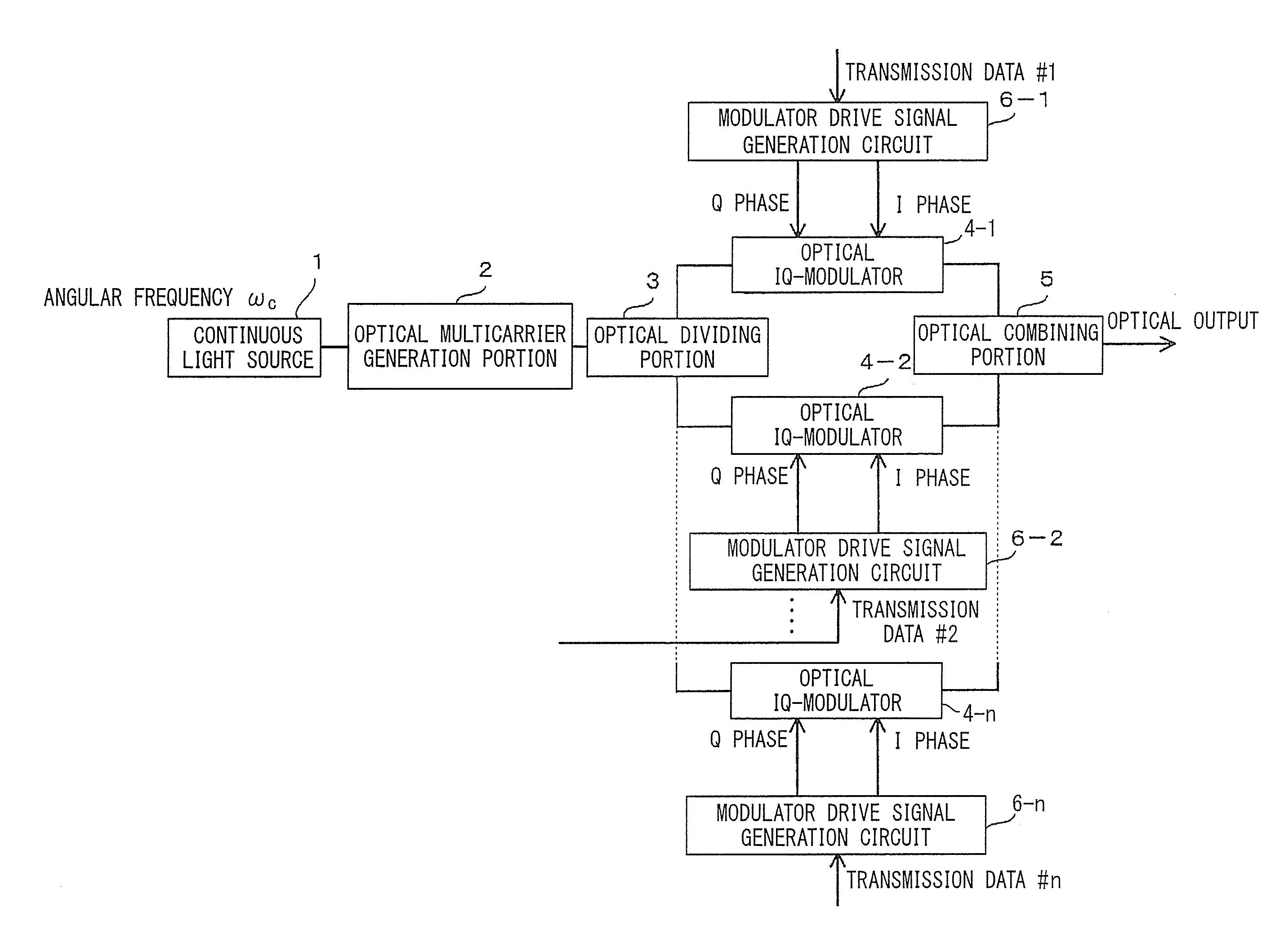
[0066]An optical modulation circuit using a multi-wavelength light source as a first embodiment of the present invention will be described with reference to FIG. 1 to FIG. 4B.

[0067]In the present embodiment, the multi-wavelength light source is made of a continuous light source 1 and an optical multicarrier generation portion 2.

[0068]FIG. 1 is a diagram showing a configuration of the optical modulation circuit of the present embodiment. As shown in FIG. 1, the optical modulation circuit of the present embodiment includes: a continuous light source 1 for outputting continuous light with an angular frequency of ωc with a constant power; an optical multicarrier generation portion 2 for generating n (n≧2) optical multicarriers from an optical carrier emitted from the continuous light source 1; an optical dividing portion 3 for dividing the optical multicarriers according to their wavelength; optical IQ-modulators 4-1 to 4-n for generating optical subcarriers in which pha...

Example

Second Embodiment

[0083]A second embodiment of the present invention will be described with reference to FIG. 5 to FIG. 8. In the present embodiment, the description is for the case where the distance between the optical subcarriers is equal to the symbol rate of the optical subcarriers.

[0084]FIG. 5 is a diagram showing a configuration of an optical transmission system of the present embodiment. The optical IQ-modulators 4-1 and 4-2, the optical multicarrier generation portion 2, and the modulator drive signal generation circuit 6-1 and 6-2 in the optical transmitter 20 of the present embodiment are configured similarly to those in the first embodiment, which are shown in FIG. 1 and FIG. 3. In this configuration, it is possible to superimpose phase-shift keying on each optical subcarrier. In the present embodiment, quaternary differential phase-shift keying (DQPSK) is employed.

[0085]It is assumed that the bit rate of the data #1 and the data #2 that are respectively input to the modu...

Example

Third Embodiment

[0094]An optical modulation circuit of a third embodiment of the present invention will be described with reference to FIG. 9 and FIG. 10. In the second embodiment, the description has been for the case where a plurality of optical subcarriers on which differential phase-shift keying (DQPSK) is employed are generated. However, in the third embodiment, the case where phase-shift keying is superimposed on a plurality of optical subcarriers will be described.

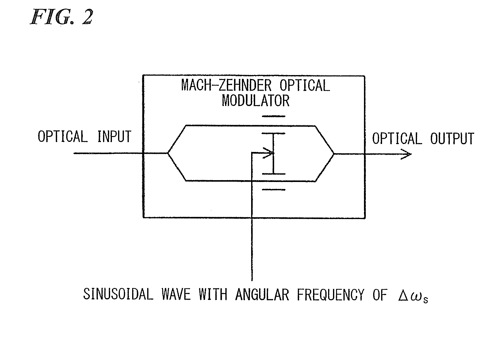
[0095]The optical modulation circuit of the third embodiment has a configuration that includes: a continuous light source 1 for outputting continuous light with a constant power; an optical IQ-modulator 4 for generating subcarriers on which phase-shift keying is employed; and a modulator drive signal generation circuit 6 for generating a modulator drive signal from data, as shown in FIG. 9. A configuration of the modulator drive signal generation circuit 6 is shown in FIG. 10.

[0096]An optical carrier with an angular...


PUM


Abstract

An optical modulator and an optical transmission system convert continuous light of a multiple wavelength light source, which generates the continuous light with a fixed and complete phase but different frequencies, to a modulator driving signal so as to generate a light subcarrier with each frequency at the center and modulate the continuous light to the light subcarrier by using the modulator driving signal. In the case where an optical modulation is carried out by an optical IQ-modulator, transmitting data, for example, is converted to two parallel data A(t) and B(t), an I phase signal, in which the data A(t)+B(t) are modulated with a clock signal with a frequency ω, and a Q phase signal, in which the data A(t)−B(t) are modulated with a clock signal with a π/2 phase shifted, are generated, and the I phase signal and the Q phase signal are applied to electrodes of the optical IQ-modulator, respectively.

Description

TECHNICAL FIELD[0001]The present invention relates to a multicarrier modulation technique for transmitting binary data in a plurality of subcarriers.[0002]Priority is claimed on Japanese Patent Application No. 2007-177871, filed on Jul. 6, 2007, the contents of which are incorporated herein by reference.BACKGROUND ART[0003]As a technique for providing a large capacity in optical fiber transmission, the wavelength division multiplexing (WDM) technique is used in which a symbol rate for a single carrier is increased to narrow the channel spacing for an increased number of multiplexes, to thereby achieve an enlarged transmission capacity.[0004]However, an increase in symbol rate results in a more noticeable influence of a chromatic dispersion and a polarization mode dispersion (PMD) in a transmission fiber. Therefore, a sophisticated compensation technique is required. In addition, in order to obtain necessary receiver sensitivity, more power is required. This leads to a problem of sup...

Claims


Application Information

Patent Timeline
IPC IPC(8): G02B26/00H04B10/2507H04B10/2513H04B10/2543H04B10/40H04B10/50H04B10/516H04B10/548H04B10/572H04B10/58H04B10/60H04B10/61
CPCG02F1/0327G02F1/225H04B10/548H04B10/5561H04B10/5053
Inventor KOBAYASHI, TAKAYUKISANO, AKIHIDEMIYAMOTO, YUTAKA
Owner NIPPON TELEGRAPH & TELEPHONE CORP
Why Eureka
Try Eureka