
Eureka
For R&D, Eureka makes reading and utilizing patents & technical documents easy.
Eureka AIR
Designed for self-driven R&D workflows. Generate viable solutions, solve complex R&D challenges, empower your innovation with AI.

Eureka Materials
Designed for material experts only. Revolutionize your material R&D, from search, analyze, to developing new materials.

TechResearch
Generate reliable direction feasibility study reports for your R&D in just a few steps.

TechSeek
Discover and master advanced knowledge NOW. Basics, ideas, possibilities, all at once.

TechMind
As an expert in R&D Theories, TechMind can generates customized viable solutions instantly.

TechRisk
Analyze your overall solution with one click, know your potential R&D risks in advance.

TechMonitor
Get weekly tech updates, stay abreast of the latest tech innovations and key insights.
Package substrate with a cavity, semiconductor package and fabrication method thereof
- Summary
- Abstract
- Description
- Claims
- Application Information
AI Technical Summary
Benefits of technology
Problems solved by technology
Method used
Image

Examples
Embodiment Construction
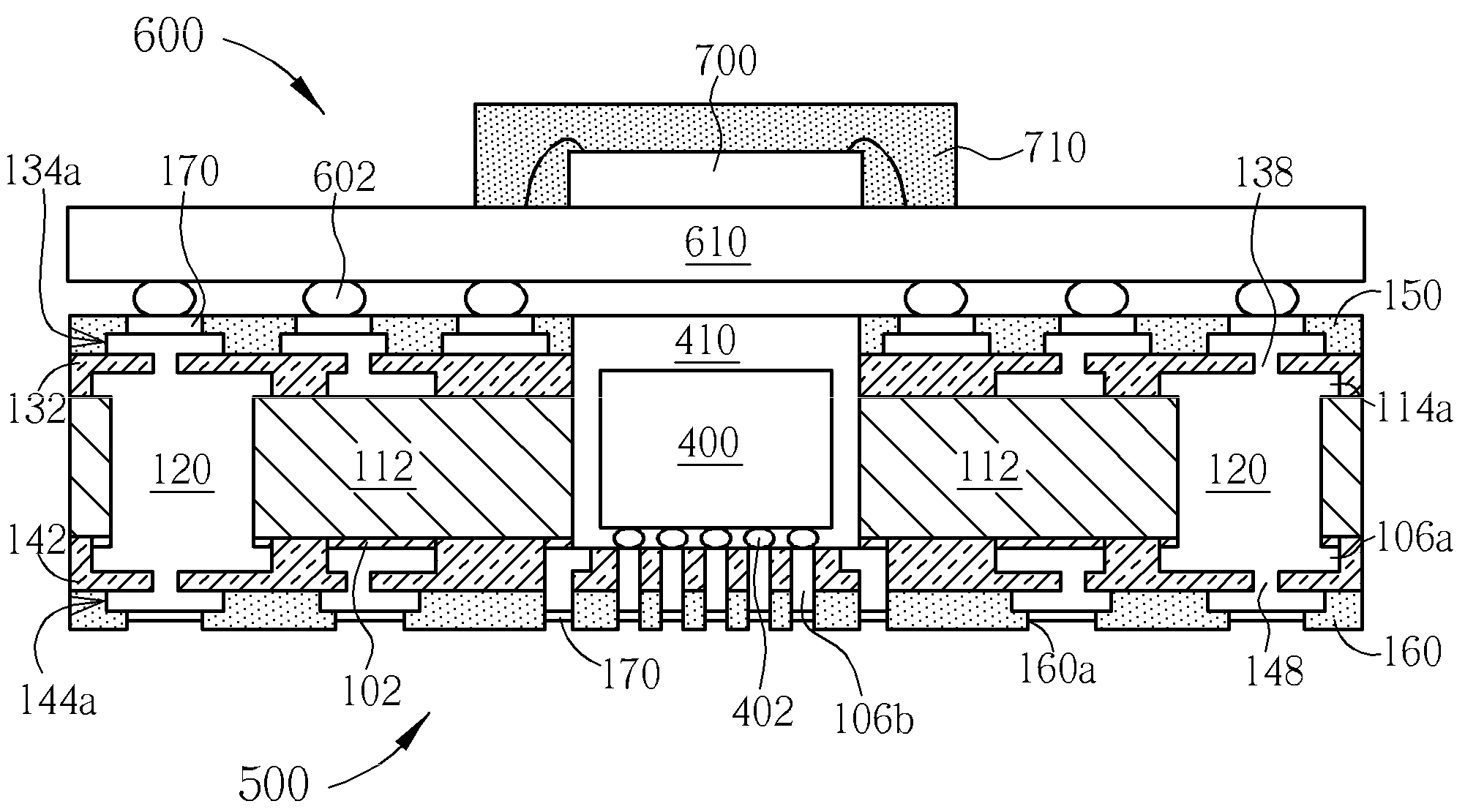
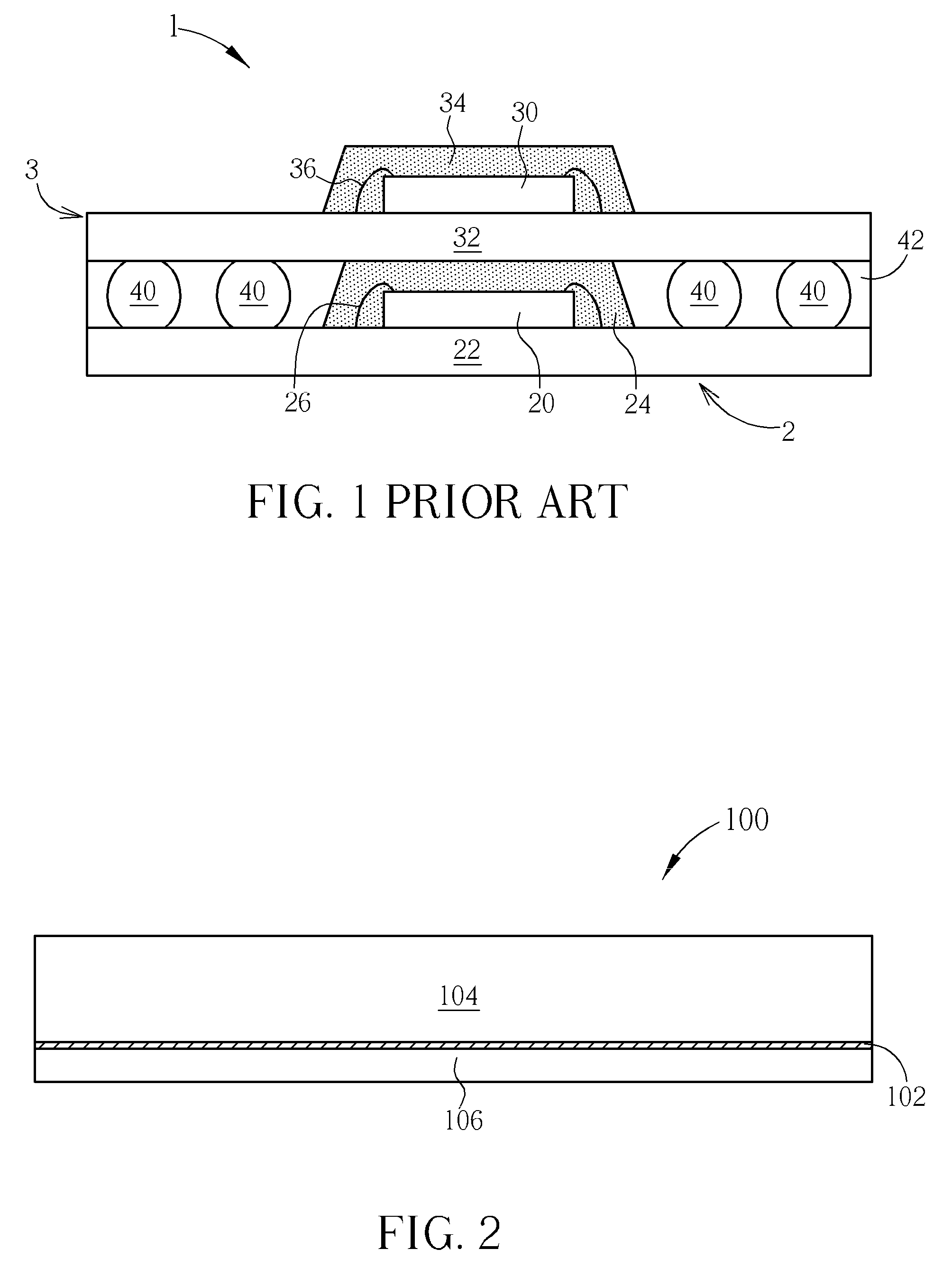
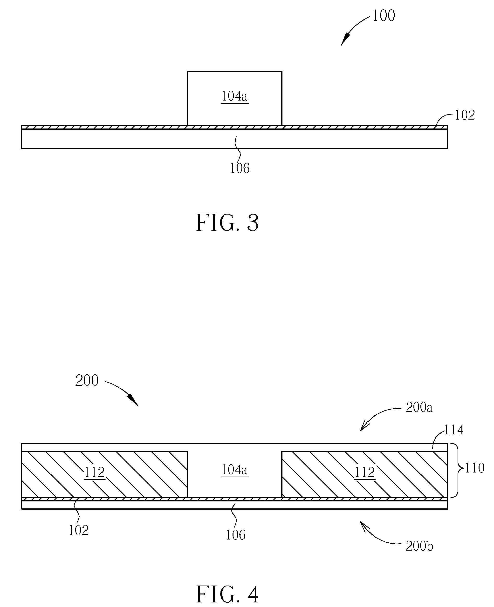
[0017]Please refer to FIG. 2 to FIG. 13. FIG. 2 to FIG. 13 are schematic, cross-sectional diagrams illustrating a process of fabricating a package-on-package structure in accordance with one preferred embodiment of this invention. First, as shown in FIG. 2, a cladding sheet 100 such as a Cu—Ni—Cu composite metal substrate, a Cu—Al—Cu composite metal substrate or a copper clad laminate (CCL) is provided. The cladding sheet 100 comprises an intermediate layer 102, a first metal layer 104 laminated on the first side of the intermediate layer 102, and a second metal layer 106 laminated on the second side opposite to the first side of the intermediate layer 102. Preferably, the first metal layer 104 is made of copper and has a thickness of about, for example, 30-150 micrometers. The thickness of the first metal layer 104 is greater than that of the second metal layer 106. Preferably, the second metal layer 106 is made of copper and has a thickness of about 1-50 micrometers. In a case tha...
PUM
| Property | Measurement | Unit |
|---|---|---|
| aaaaa | aaaaa |
Abstract
Description
Claims
Application Information
 - R&D Engineer
- R&D Manager
- IP Professional
- Industry Leading Data Capabilities
- Powerful AI technology
- Patent DNA Extraction
Browse by: Latest US Patents, China's latest patents, Technical Efficacy Thesaurus, Application Domain, Technology Topic, Popular Technical Reports.
© 2024 PatSnap. All rights reserved.Legal|Privacy policy|Modern Slavery Act Transparency Statement|Sitemap|About US| Contact US: help@patsnap.com