

Electroluminescent device
a technology of electroluminescent devices and electrodes, which is applied in the direction of luminescent compositions, organic semiconductor devices, luminescent compositions, etc., can solve the problems of limiting the possibility of recombination of electrons and holes, quantum dots that are easily coagulated in their dispersion, and the mobility of excitons is improved. , the effect of excellent luminous efficiency
- Summary
- Abstract
- Description
- Claims
- Application Information
AI Technical Summary
Benefits of technology
Problems solved by technology
Method used
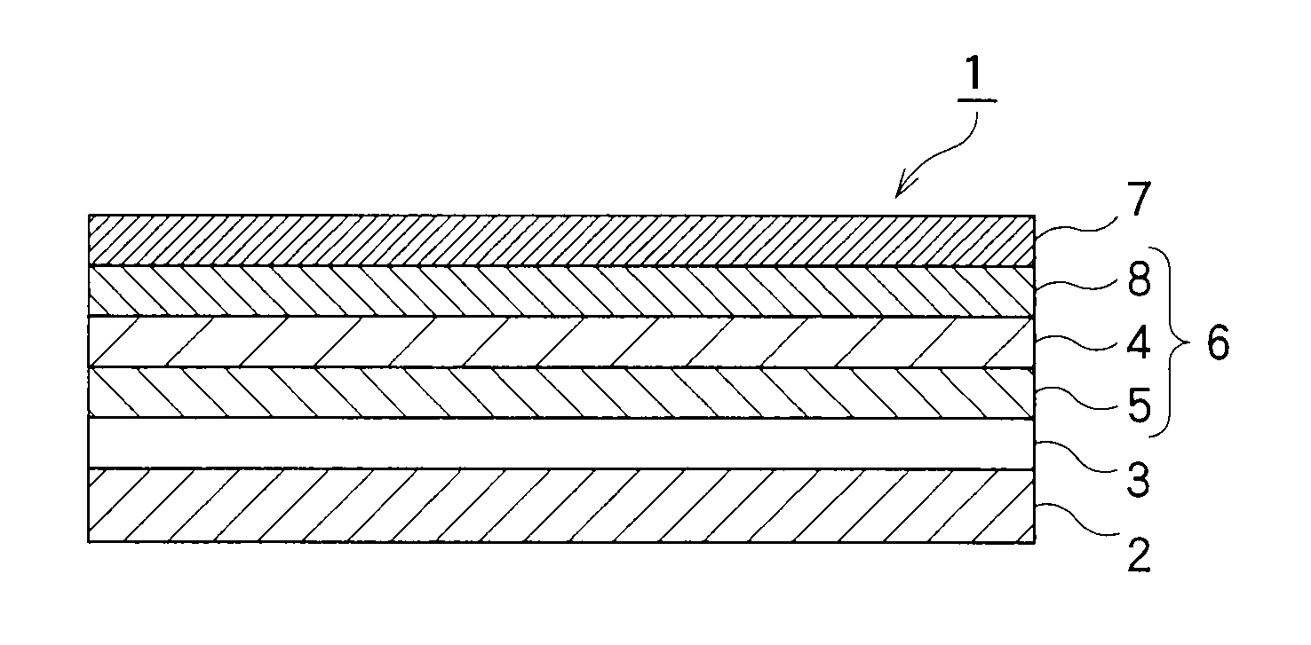
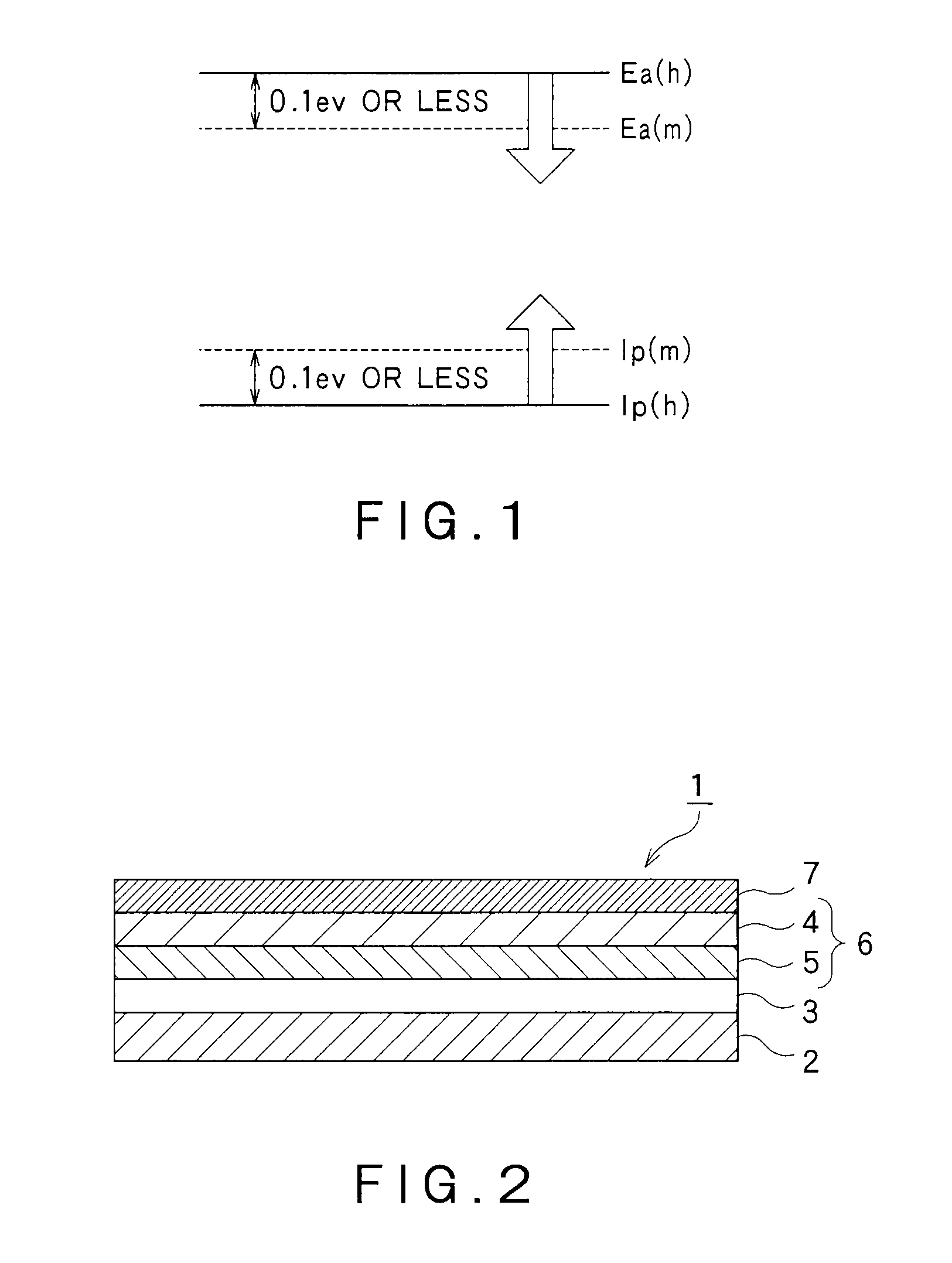
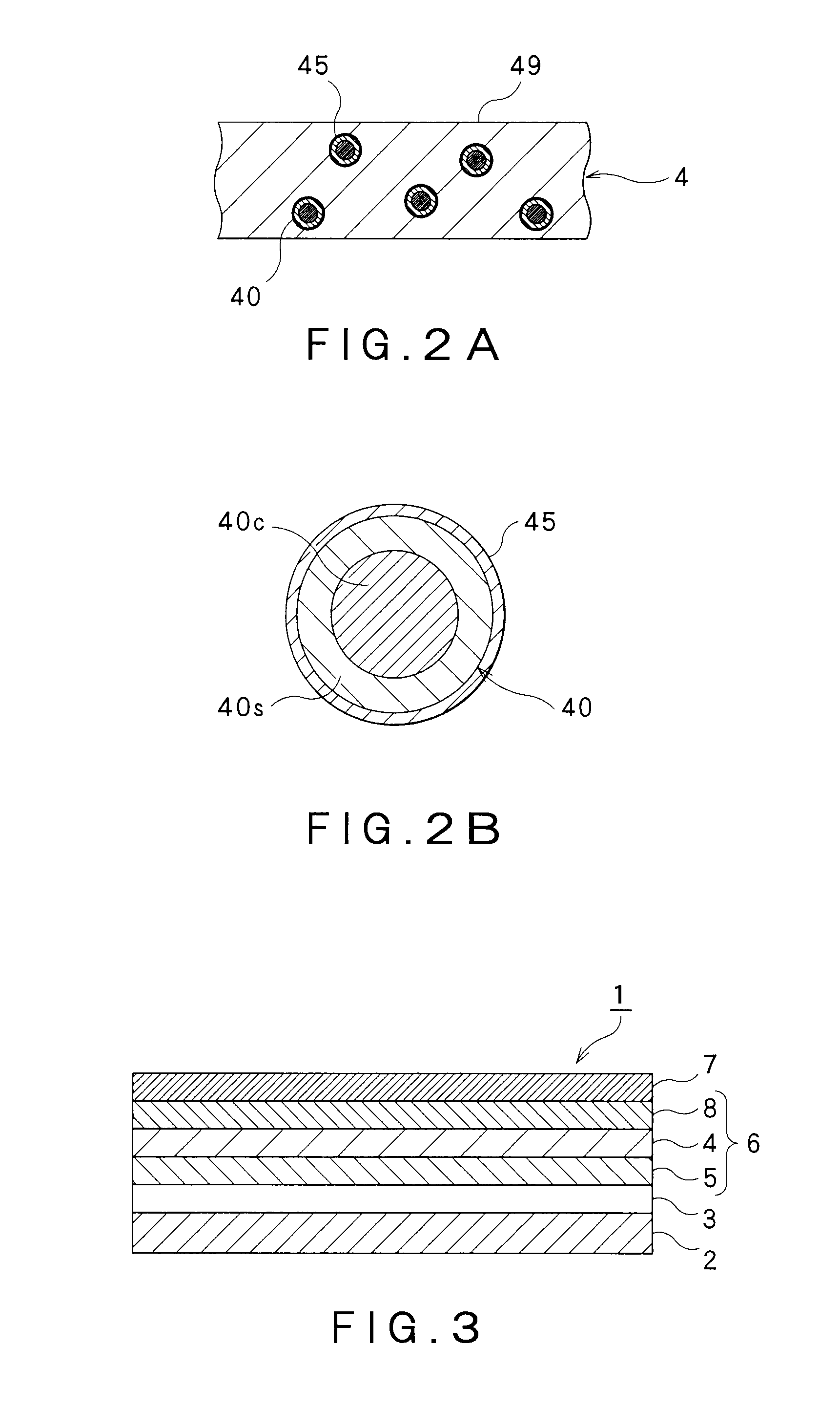
Image

Examples
synthesis example 1
(Synthesis Example 1)
[0204]A compound (formula (1)) was synthesized by adding, as the hydrophilic group, a group having phosphine oxide to the benzothiazole group in 3-(2-benzothiazolyl)-7-(diethylamino)coumarin [Coumarin 6: Ea=3.2 eV, Ip=5.5 eV, Eg=2.3 eV, molecular weight 350]. (The compound is referred to as CAP-1a.)
synthesis example 2
(Synthesis Example 2)
[0205]A compound (formula (2 )) was synthesized by adding, as the hydrophilic group, a group having phosphine oxide to the tetraphenyl group in 5,6,11,12-tetraphenylnaphthacene [rubrene: Ea=3.2 eV, Ip=5.4 eV, Eg=2.2 eV, molecular weight 533]. (The compound is referred to as CAP-1b.)
synthesis example 3
(Synthesis Example 3)
[0206]A compound (formula (3)) was synthesized by adding, as the hydrophilic group, a group having phosphine oxide to the butyl group in 2,5,8,11-tetra-tert-butylperilene [TBPe: Ea=3.2 eV, Ip=5.9 eV, Eg=2.7 eV, molecular weight 488]. (The compound is referred to as CAP-1c.)
[0207][Synthesis of Second Protective Materials (Protective Materials for Charge Transport)]
PUM
| Property | Measurement | Unit |
|---|---|---|
| emission wavelength | aaaaa | aaaaa |
| emission wavelength | aaaaa | aaaaa |
| particle diameters | aaaaa | aaaaa |
Abstract
Description
Claims
Application Information