

Light-emitting element, light-emitting device, display, and electronic apparatus
a technology of light-emitting devices and light-emitting elements, which is applied in the direction of solid-state devices, semiconductor devices, thermoelectric devices, etc., can solve the problems of increasing the likely increase of the driving voltage of the light-emitting element, so as to achieve efficient light emission, efficient transfer, and efficient transfer
- Summary
- Abstract
- Description
- Claims
- Application Information
AI Technical Summary
Benefits of technology
Problems solved by technology
Method used
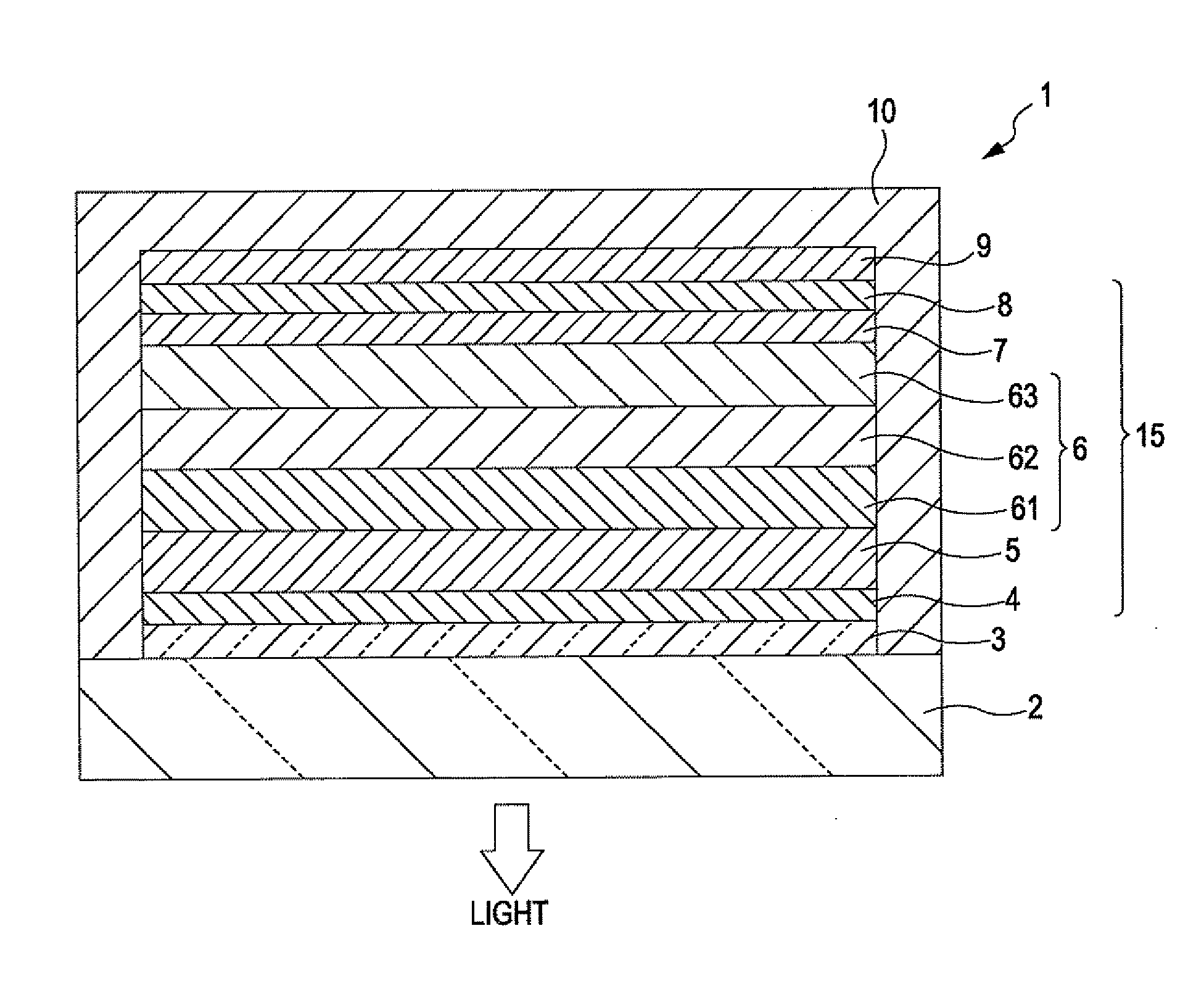
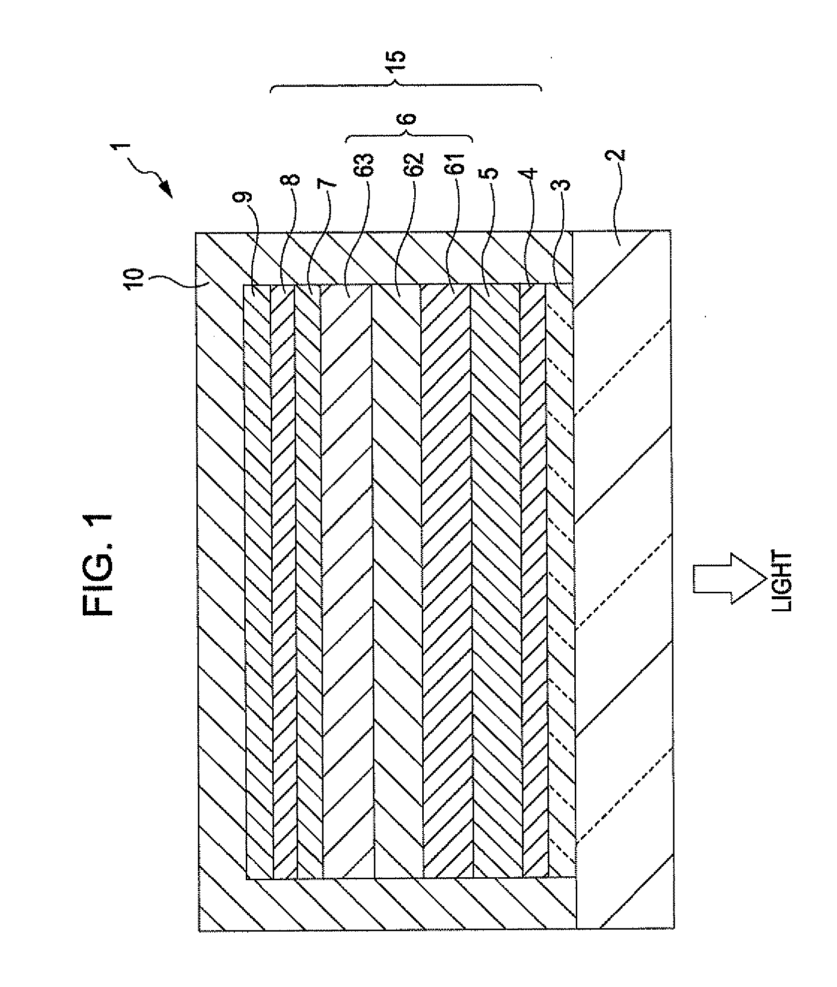
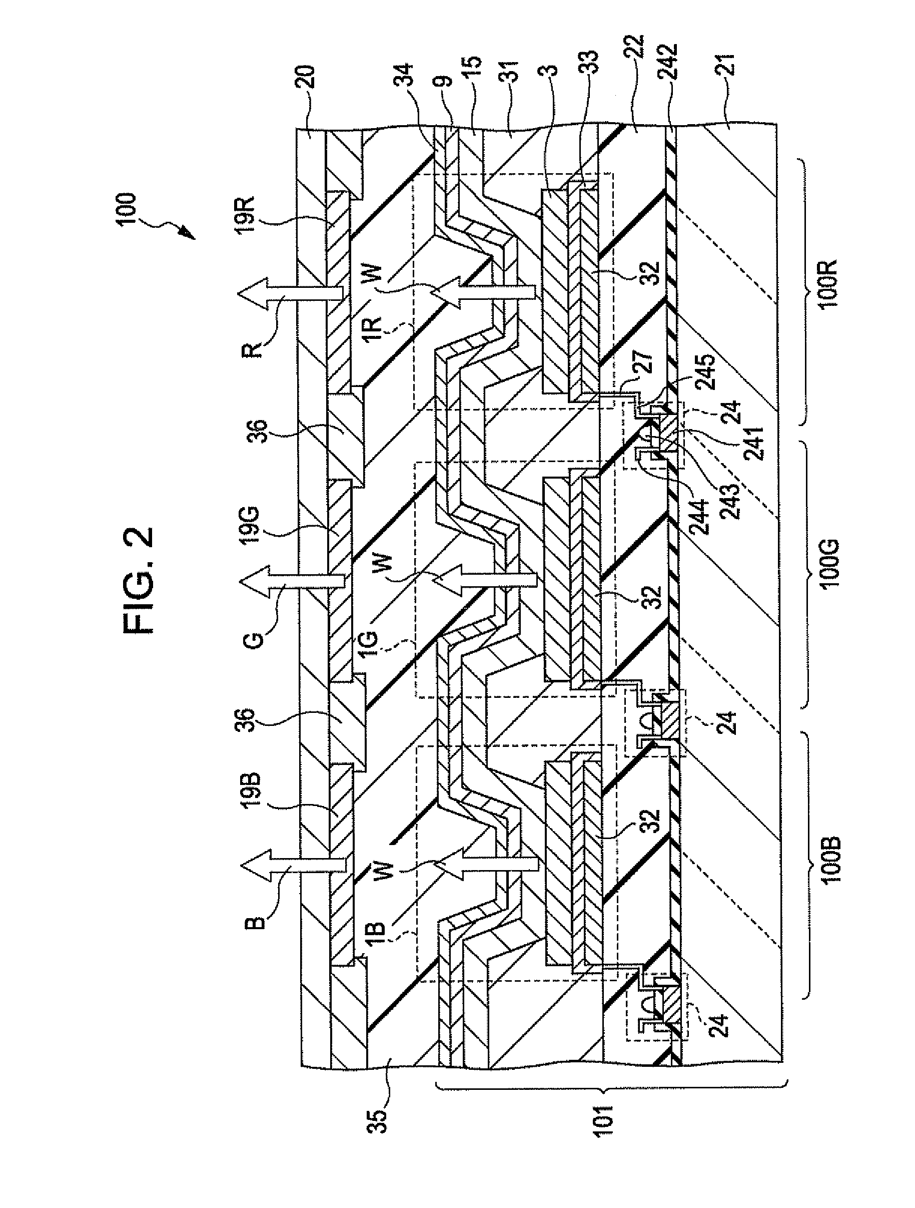
Image

Examples
example
[0186]An example of the present invention is described below in detail.
[0187]A light-emitting element was manufactured as described below.
[0188]A transparent glass substrate with an average thickness of 0.5 mm was prepared. An ITO electrode serving as an anode was formed on the glass substrate by a sputtering process so as to have an average thickness of 50 nm.
[0189]After the glass substrate was immersed in acetone and 2-propanol in that order and was ultrasonically cleaned, the glass substrate was subjected to oxygen plasma treatment.
[0190]N,N′-bis(4-diphenylamino-phenyl)-N,N′-diphenyl-biphenyl-4-4′-diamine having Formula (I) was deposited on the ITO electrode by vacuum vapor deposition, whereby a hole injection layer with an average thickness of 40 nm was formed.
[0191]N,N′-di(1-naphtyl)-N,N′-diphenyl-1,1′-diphenyl-4,4′-diamine (α-NPD) having Formula (II) was deposited on the hole injection layer by vacuum vapor deposition, whereby a hole transport layer with an average thickness o...
PUM
 Abstract
Description
Claims
Application Information