High frequency plasma CVD apparatus, high frequency plasma CVD method and semiconductor thin film manufacturing method

a plasma cvd and plasma technology, applied in the direction of coatings, chemical vapor deposition coatings, electric discharge tubes, etc., to achieve the effect of effectively solving power loss problems

Inactive Publication Date: 2010-09-23
MURATA MASAYOSHI
View PDF3 Cites 24 Cited by
  • Summary
  • Abstract
  • Description
  • Claims
  • Application Information

AI Technical Summary

Benefits of technology

[0109]Next, in the technology described in Patent Document 5, a balanced-to-unbalanced converter is arranged between the impedance matching boxes in the power supply circuit and the feeding points on the electrodes; the balanced-to-unbalanced converter and the feeding points of the pair of electrodes are short-circuited on at least both ends of the outer conductors of the two coaxial cables having the same length, one end of each core line of the tw

Problems solved by technology

The discovery of a plasma CVD apparatus and a method related to items (b) to (e) is a major issue in the design for manufacturing with good reproduc

Method used


Image

  • High frequency plasma CVD apparatus, high frequency plasma CVD method and semiconductor thin film manufacturing method
  • High frequency plasma CVD apparatus, high frequency plasma CVD method and semiconductor thin film manufacturing method
  • High frequency plasma CVD apparatus, high frequency plasma CVD method and semiconductor thin film manufacturing method

Examples


example 1

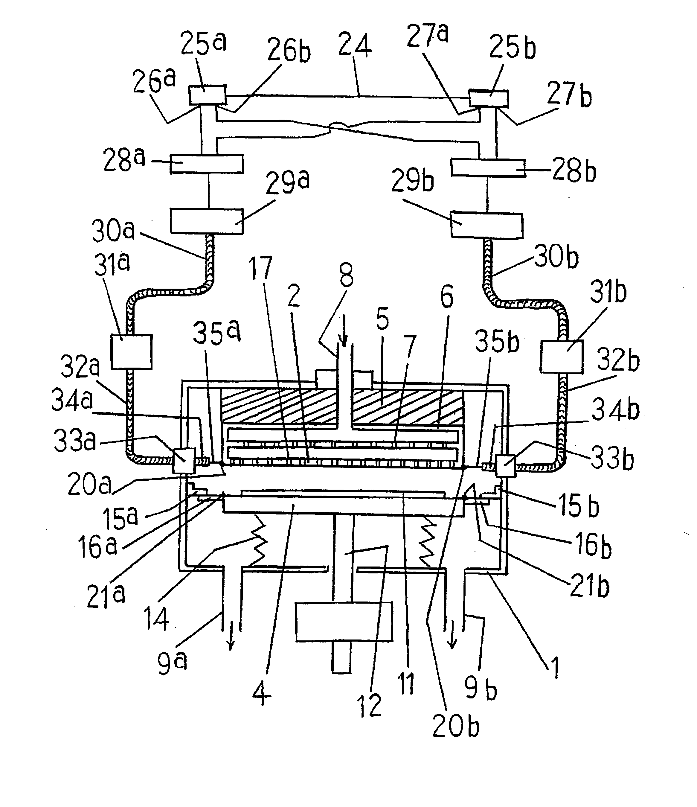
[0237]First, plasma CVD apparatus and plasma CVD method relating to the first exemplary embodiment of the present invention are explained with reference to FIGS. 1 to 8.

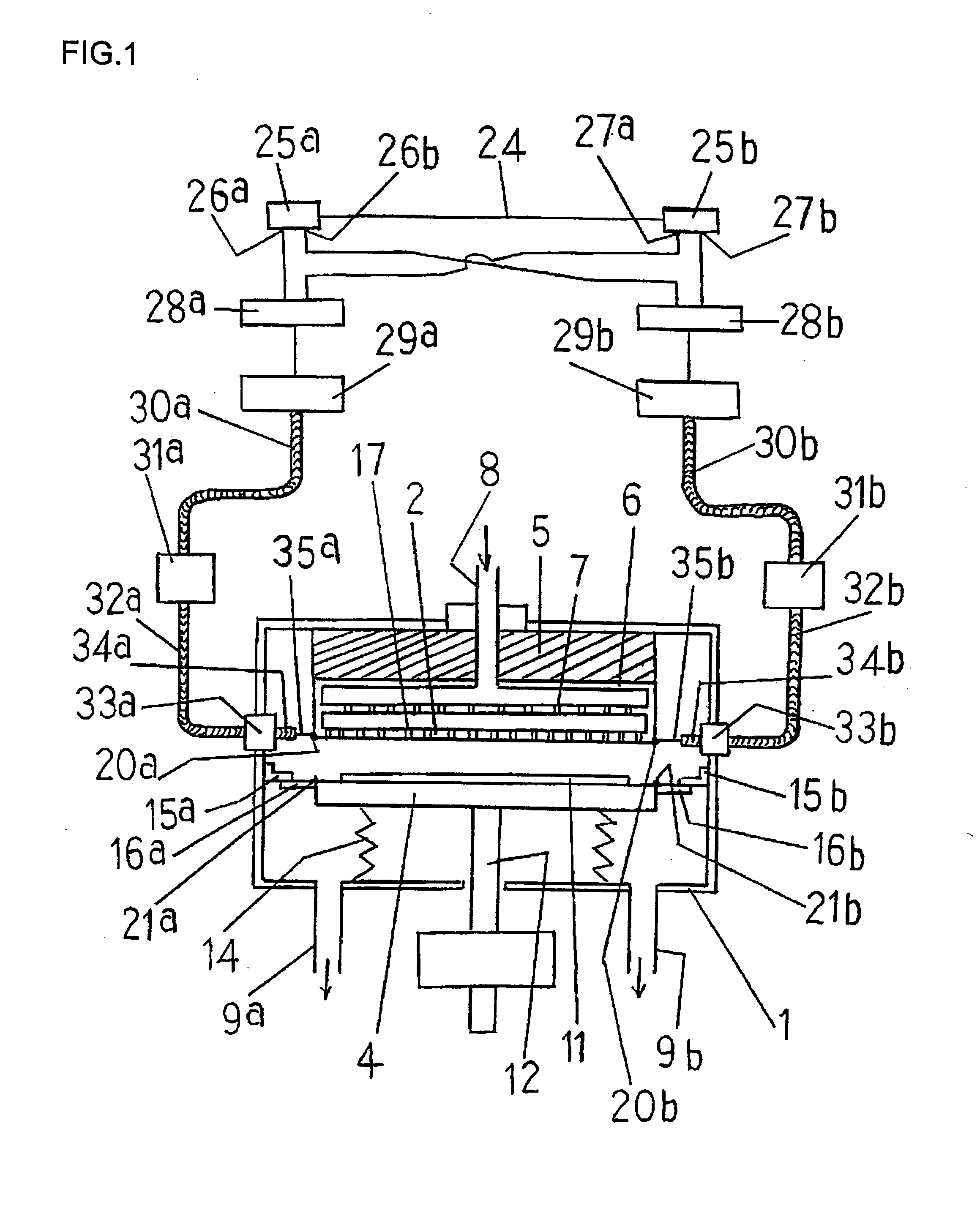
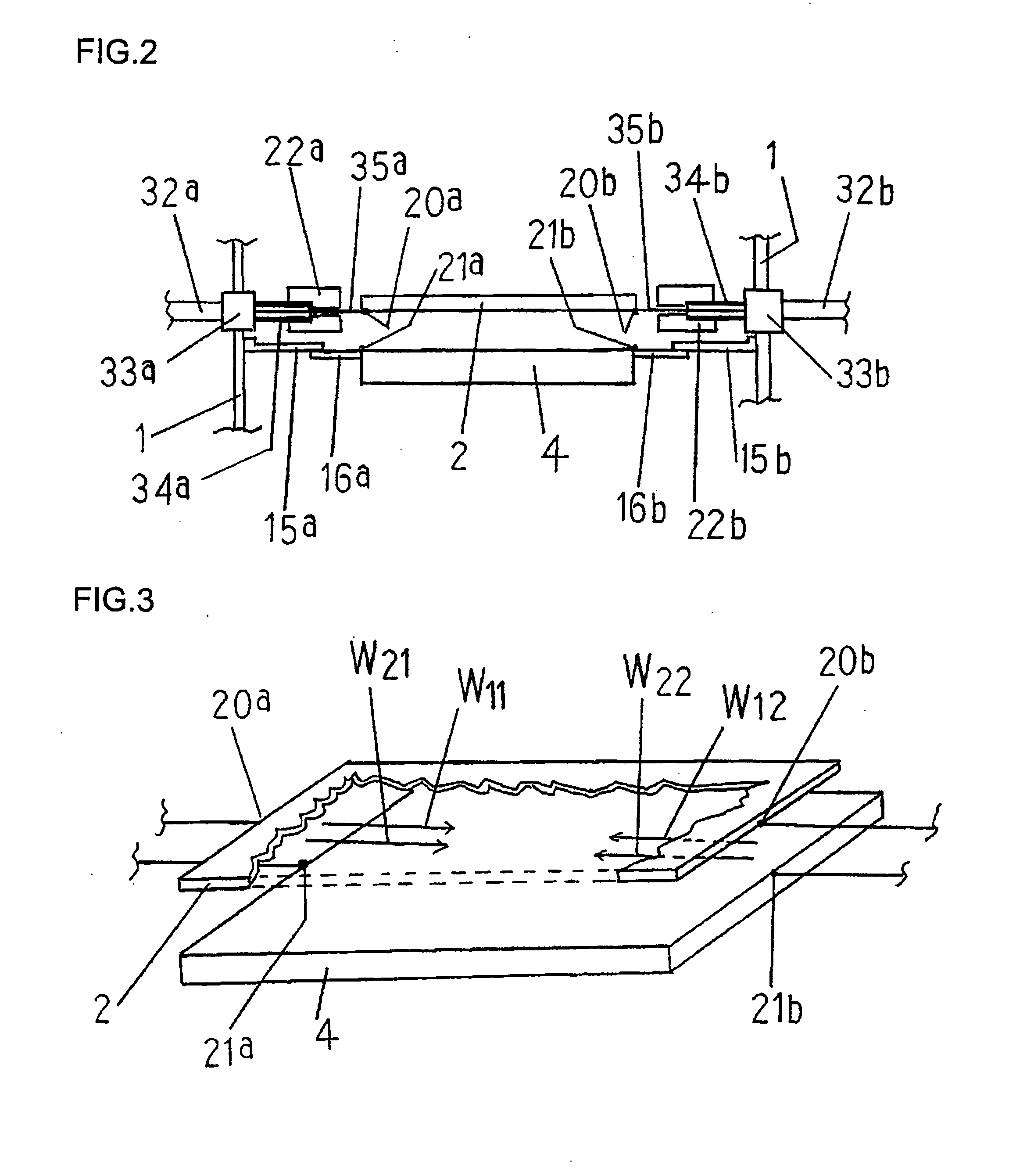
[0238]FIG. 1 is a schematic view showing the entire plasma CVD apparatus relating to the first exemplary embodiment of the present disclosure. FIG. 2 is an explanatory drawing showing the structure of the power supply unit to the pair of electrodes in the plasma CVD apparatus shown in FIG. 1. FIG. 3 is a schematic view of the transmission of power fed to the pair of electrodes in the plasma CVD apparatus shown in FIG. 1. FIG. 4 is an explanatory drawing showing the adjustment method of the power transmission when the power is supplied in the film deposition of the i-type microcrystalline silicon film using the plasma CVD apparatus shown in FIG. 1. FIG. 5 is an explanatory drawing illustrating a typical example of the pulse-modulated outputs from the 1st and the 2nd pulse-modulation, phase-adjustable, 2-output transmi...

example 2

[0411]Next, the plasma CVD apparatus and the plasma CVD method related to the second exemplary embodiment of the present disclosure are explained with reference to FIGS. 9 to 11.

[0412]FIG. 9 is an explanatory drawing showing the entire plasma CVD apparatus related to the second exemplary embodiment of the present disclosure. FIG. 10 is an explanatory drawing of the power supply apparatus to the pair of electrodes that uses a balanced-to-unbalanced converter in the plasma CVD apparatus shown in FIG. 2. FIG. 11 is an explanatory drawing of the flow of the high-frequency current in the power supply apparatus to the pair of electrodes that used the balanced-to-unbalanced converter shown in FIG. 10.

[0413]First, the constitution of the apparatus is explained. However, parts which are the same parts indicated in the plasma CVD apparatus related to the first embodiment of the present disclosure described above are assigned the same reference numbers, and their explanations are omitted.

[0414...


PUM

PropertyMeasurementUnit
Lengthaaaaaaaaaa
Frequencyaaaaaaaaaa
Timeaaaaaaaaaa

Abstract

Provided are large area and uniform VHF plasma CVD apparatus and method wherein a plasma generating source constitutes the VHF plasma CVD apparatus for manufacturing a tandem-type thin film silicon solar cell, and influences of standing waves, generation of harmful plasma other than between a pair of electrodes and supply power consumption other than between the pair of electrodes are suppressed. First and second power feed points are arranged on an electrode at positions facing each other. A distance between the power feed points is set at an integral multiple of a half of the wavelength of the using power, and a pulse power separated in terms of time is supplied. The pulse power is outputted from two phase-variable double output high frequency power supplies which can perform pulse modulation. Thus, a first standing wave wherein the anti-node position matches with positions of the first and the second power feed points, and a second standing wave wherein the node position matches with positions of the first and the second power feed points are alternately generated in terms of time.

Description

TECHNICAL FIELD[0001]The present invention relates to a high-frequency plasma CVD apparatus, high-frequency plasma CVD method, and semiconductor thin-film manufacturing method that are used in the manufacture of integrated tandem-type thin-film solar cells (termed as “tandem thin-film solar cells”, hereafter), in particular, to a VHF plasma CVD apparatus and VHF plasma CVD method, where the frequency is 30 MHz to 300 MHz (VHF band).[0002]In addition, the present invention relates to a high-frequency plasma CVD apparatus and a high-frequency plasma CVD method used in the manufacture of various apparatuses that apply micro-nano-crystalline (termed generally as “microcrystalline” herein) silicon=film and crystalline silicon film.BACKGROUND AND DISCUSSION THEREOF[0003]In a multi-junction photoelectric conversion element that laminates a plurality of semiconductor photoelectric conversion units having a photoelectric conversion function, the combination of a top cell and a bottom cell ha...

Claims


Application Information

Patent Timeline
IPC IPC(8): C23C16/00
CPCC23C16/24H01J37/32091C23C16/509
Inventor MURATA, MASAYOSHI
Owner MURATA MASAYOSHI
Why Eureka
Try Eureka