
Dicing die-bonding film

a die-bonding film and die-bonding technology, applied in the direction of film/foil adhesives, synthetic resin layered products, transportation and packaging, etc., can solve the problems of long time, special equipment, and difficulty in uniform adhesive layer, and achieve the effect of further improving the pick-up property

Inactive Publication Date: 2010-09-23
NITTO DENKO CORP
View PDF20 Cites 18 Cited by
  • Summary
  • Abstract
  • Description
  • Claims
  • Application Information

AI Technical Summary

Benefits of technology

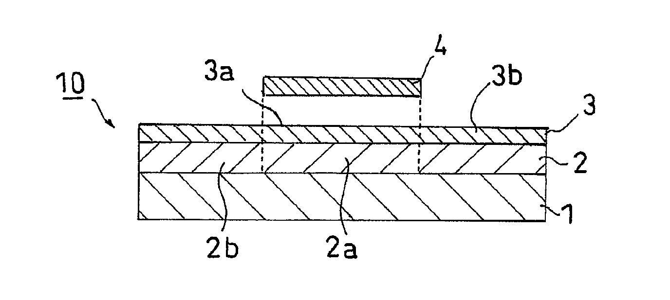
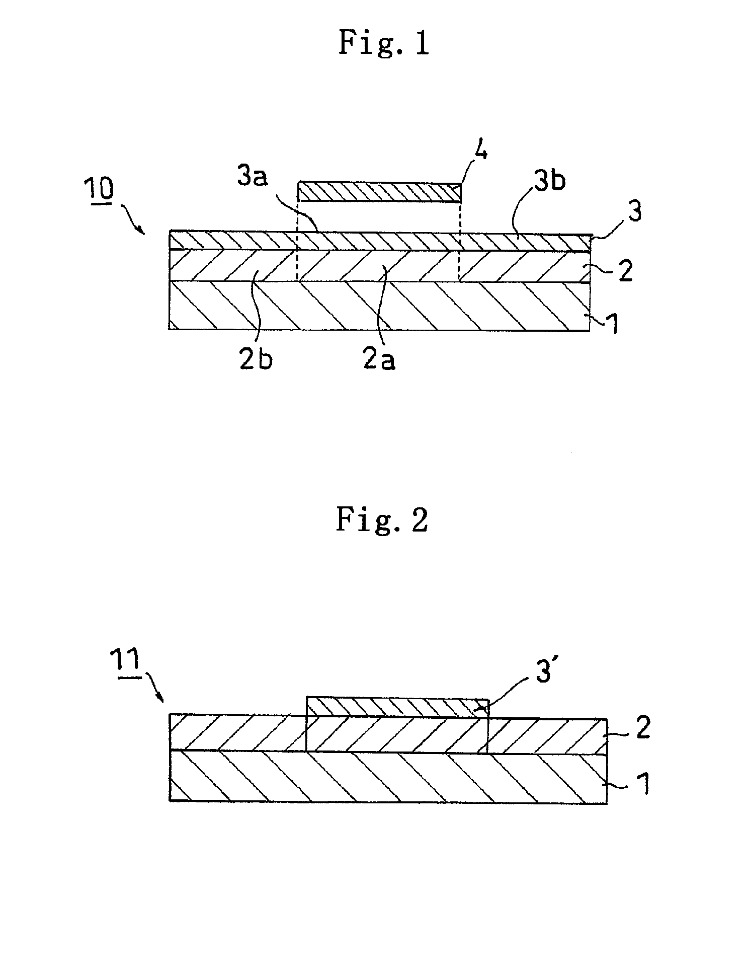
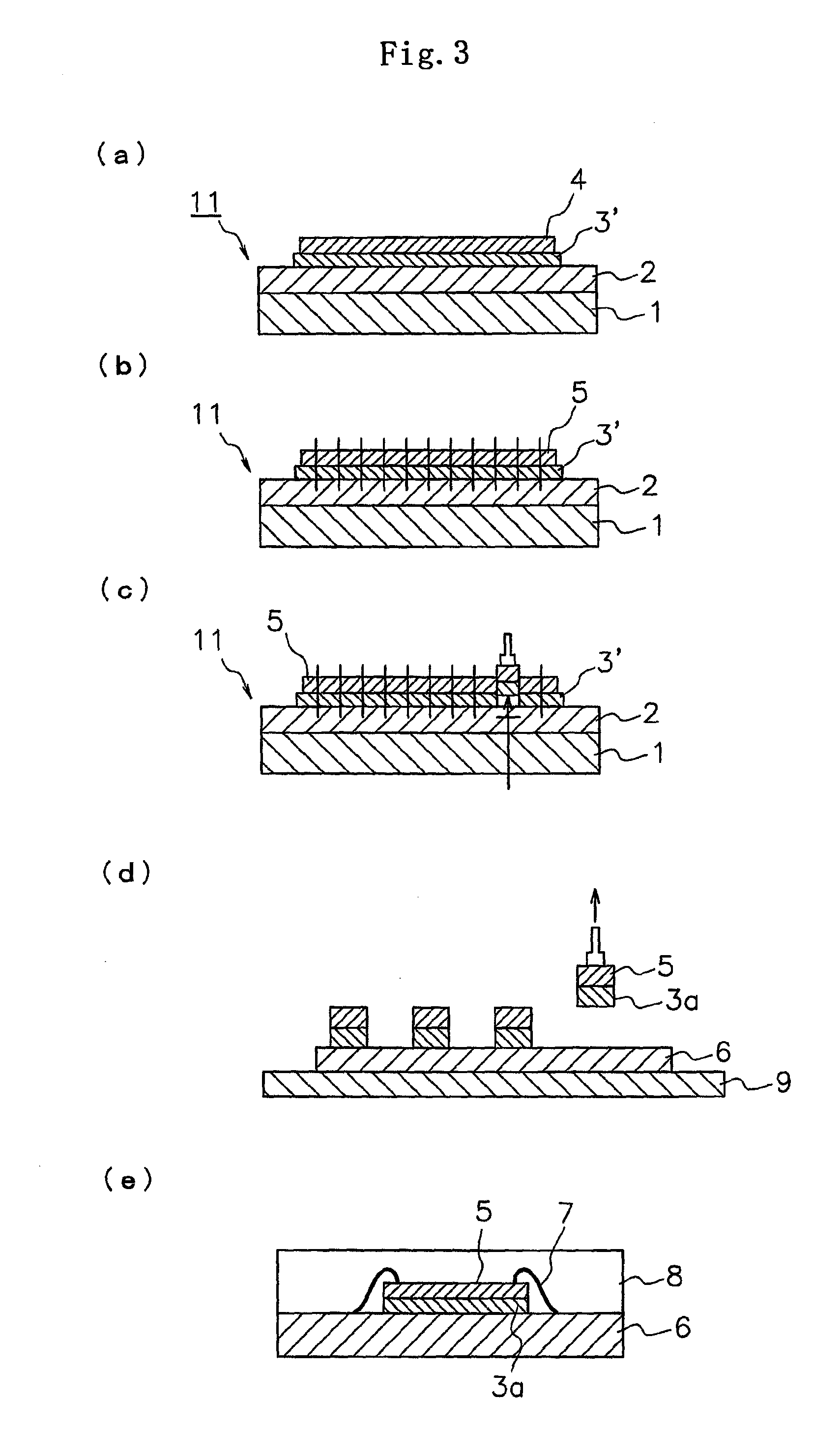
[0010]The dicing film of the present invention contains, as an essential component, a crosslinking agent having two or more functional groups having reactivity with a hydroxyl group in the molecule. By controlling the additive amount of this crosslinking agent, a tensile elastic modulus is adjusted so as to make it possible to achieve good pickup property while maintaining holding strength during dicing. Since the content of the crosslinking agent of the present invention is 2 parts by weight or more based on 100 parts by weight of the polymer, it is possible to suppress insufficient crosslinking after ultraviolet irradiation and to prevent an adhesive residue from generating to a dicing ring to be stuck on the pressure-sensitive adhesive layer during dicing. It is also possible to prevent deterioration of pickup property of a semiconductor chip. On the other hand, since the content is 20 parts by weight or less, it is possible to prevent chipping during dicing.
[0011]Also, insufficient crosslinking after ultraviolet irradiation is suppressed by adjusting the content of a hydroxyl group-containing monomer to 10 mol % or more. As a result, it is possible to prevent an adhesive residue from generating to a dicing ring to be stuck on the pressure-sensitive adhesive layer during dicing. On the other hand, when the content of a hydroxyl group-containing monomer is adjusted to 30 mol % or less, it is possible to prevent deterioration of pickup property caused by that polarity of the pressure-sensitive adhesive increases and thus interaction with the die-bonding film increases to make it difficult to perform peeling.
[0012]In the present invention, since the isocyanate compound having a radical reactive carbon-carbon double bond is employed in place of a polyfunctional monomer, the polyfunctional monomer is not diffused in the die-bonding film. As a result, it is made possible to prevent the boundary surface between the dicing film and the die-bonding film from being disappeared and to achieve better pickup property.
[0015]It is preferable that the pressure-sensitive adhesive layer does not contain acrylic acid. Whereby, the reaction and interaction between the pressure-sensitive adhesive layer and the die-bonding film can be prevented and pickup property can be further improved.

Problems solved by technology

However, with this method, it is difficult to make the adhesive layer uniform and a special apparatus and a long period of time become necessary in the application of the adhesive.
However, it has never been easy to balance both characteristics.
Especially when a large holding strength is required in the adhesive layer such as in a method of dicing a semiconductor wafer with a rotary circular blade, or the like, it is difficult to obtain a dicing die-bonding film that satisfies the above-described characteristics.
However, there is the case where a dicing die-bonding film that is excellent in balance between holding strength during dicing and peeling property after dicing is hardly obtained even by this modification method.
For example, when a large semiconductor chip measuring 10 mm×10 mm or more is to be obtained, it is not easy to pickup the semiconductor chip using a common die bonder because of the large area thereof.

Method used


Image

  • Dicing die-bonding film
  • Dicing die-bonding film
  • Dicing die-bonding film

Examples


example 1

Manufacture of Dicing Film

[0094]An acryl polymer A was obtained by charging 86.4 parts of 2-ethylhexylacrylate (hereinbelow, refers to as “2EHA”), 13.6 parts of 2-hydroxyethylacrylate (hereinbelow, referred to as “HEA”), 0.2 parts of benzoylperoxide, and parts of toluene into a reactor equipped with a condenser, a nitrogen introducing pipe, a thermometer, and a stirring apparatus, and performing a polymerization process at 61° C. for 6 hours in a nitrogen flow. The HEA was 20 mol %.

[0095]An acryl polymer A was obtained by adding 14.6 parts of 2-methacryloyloxyethylisocyanate (hereinbelow, referred to as “MOI”) (80 mol % to HEA) to the acryl polymer A and performing an addition reaction process at 50° C. for 48 hours in an air flow.

[0096]Next, a pressure-sensitive adhesive solution was manufactured by adding 8 parts of a polyisocyanate compound (trade name: COLONATE L, manufactured by Nippon Polyurethane Industry Co., Ltd.) and 5 parts of a photopolymerization initiator (trade name: ...

examples 2 to 9

[0101]A dicing die-bonding film was manufactured in each of examples 2 to 9 in the same manner as in the example 1 except that the composition and the content were changed to the values shown in Table 1 below.

TABLE 1Hydroxylgroup-containingIsocyanateCrosslinkingmonomercompoundagentPhotopolymerization2EHAHEA4HBAMOIAOIC / LC2030initiatorExample 186.413.6—14.6—8—5(20)(80)Example 293.5 6.6— 7.9—8—5(10)(90)Example 378.721.3—22.7—8—5(30)(80)Example 486.413.6—12.3—8—5(20)(70)Example 584—1614.2—8—5(20)(80)Example 686.413.6—13.48—5(20)(80)Example 786.413.614.6—4—5(20)(80)Example 886.413.614.6—16—5(20)(80)Example 986.413.614.6——85(20)(80)The numerical value in parentheses represents “mol”, while the numerical value in parentheses in MOI and AOI represents “molar ratio” to HEA or 4HBA.

[0102]The meanings of abbreviations described in Table 1 and Table 2 mentioned hereinafter are as follows.[0103]2EHA: 2-ethylhexyl acrylate[0104]HEA: 2-hydroxyethyl acrylate[0105]4HBA: 4-hydroxybutyl acrylate[0106]...


PUM

PropertyMeasurementUnit
Percent by massaaaaaaaaaa

Abstract

The present invention provides a dicing die-bonding film having a pressure-sensitive adhesive layer on a base material, and a die-bonding film formed on the pressure-sensitive adhesive layer. A dicing die-bonding film having a dicing film having a pressure-sensitive adhesive layer on a base material, and a die-bonding film formed on the dicing film, wherein the pressure-sensitive adhesive layer contains a polymer that is obtained by the addition-reaction of an acrylic polymer containing 10 to 30 mol % of a hydroxyl group-containing monomer with 70 to 90 mol % of an isocyanate compound having a radical reactive carbon-carbon double bond based on the hydroxyl group-containing monomer, and also contains 2 to 20 parts by weight of a crosslinking agent containing two or more functional groups having reactivity with a hydroxyl group in the molecule based on 100 parts by weight of the polymer, and the die-bonding film comprises an epoxy resin.

Description

TECHNICAL FIELD[0001]The present invention relates to a dicing die-bonding film that is used for dicing a workpiece by providing an adhesive for fixing a chip-shaped workpiece (such as a semiconductor chip) and an electrode member onto the workpiece (such as a semiconductor wafer) before dicing.BACKGROUND ART[0002]A semiconductor wafer (workpiece) in which a circuit pattern is formed is diced into semiconductor chips (chip-shaped workpiece) (a dicing step) after the thickness thereof is adjusted as necessary by backside polishing. In the dicing step, the semiconductor wafer is generally washed with an appropriate liquid pressure (normally, about 2 kg / cm2) in order to remove a cutting layer. The semiconductor chip is then fixed onto an adherend such as a lead frame with an adhesive (a mounting step), and then transferred to a bonding step. In the mounting step, the adhesive has been applied onto the lead frame or the semiconductor chip. However, with this method, it is difficult to m...

Claims


Application Information

Patent Timeline
IPC IPC(8): B32B27/08C09J7/38
CPCC08L63/00C09J7/0207H01L2924/0665H01L2924/01006H01L2224/2919H01L2221/68377H01L2221/68327H01L21/6836C09J133/066C09J2201/606C09J2203/326C09J2475/00C08L2666/22H01L2924/00H01L2924/181C09J7/38Y10T428/31511C09J2301/302H01L2924/00012C09J7/22H01L24/27H01L24/29H01L24/83H01L24/97H01L24/48H01L24/85
Inventor MATSUMURA, TAKESHIKAMIYA, KATSUHIKOMURATA, SHUUHEI
Owner NITTO DENKO CORP
Learn More