Apparatus for surface-treating wafer using high-frequency inductively-coupled plasma

a technology of inductively coupled plasma and surface treatment, which is applied in the direction of electric discharge tubes, chemical vapor deposition coatings, coatings, etc., can solve the problems of not being able to maintain constant plasma, no high-frequency power is transferred to the dielectric window, and several developed plasma treatment apparatuses are limitedly used. to achieve the effect of preventing the deterioration of the characteristics of the wafer and forming a process window

Inactive Publication Date: 2010-09-30
EUGENE TECH CO LTD
View PDF9 Cites 95 Cited by
  • Summary
  • Abstract
  • Description
  • Claims
  • Application Information

AI Technical Summary

Benefits of technology

[0013]As described above, the apparatus for surface-treating a wafer using high-frequency inductively-coupled plasma according to the present invention is advantageous in that in order to treat the surface of a wafer using plasma in oxidation, nitridation, deposition and etching processes, the helical type high-frequency plasma generated from the plasma generation unit is supplied to the wafer treatment unit for treating the wafer together with a reaction gas, thus realizing a process chamber which can be used to easily form a process window.
[0014]Further, the apparatus for surface-treating a wafer using high-frequency inductively-coupled plasma according to the present invention is advantageous in that since the components surrounding the process chamber are formed of nonconductive materials, they prevent plasma from being directly applied to the wafer, thus preventing the deterioration in the characteristics of the wafer due to physical and chemical imbalance of the wafer, and in that since diffusion surfaces a

Problems solved by technology

This method has a serious problem in that, when electroconductive materials, such as metals, TiN, and the like, are applied on the inner surface of the dielectric windows, none of the high-frequency power is transferred to the dielectric window, and thus plasma cannot be maintained constant.
Therefore, currently, several developed plasma treatment apparatuses are also limitedly used only in dielectric thin film processes etc.
Further, they are problematic in that the interior dielectric material must be continuously cleaned for maintenance and in that when the dielectric window is fabricated in a large size, the mechanical strength of the dielectric window may be decreased and there is a difficulty in the maintenance, thus causing the application to the fabrication of a large-sized dielectric window to difficult.
Although this method is advantageous in that the surface of the wafer is not damaged by plasma because the plasma generated during a process is filtered or does not influence the surface thereof, this method is problematic in that since microwaves are used as the plasma source, proce

Method used


Image

  • Apparatus for surface-treating wafer using high-frequency inductively-coupled plasma
  • Apparatus for surface-treating wafer using high-frequency inductively-coupled plasma
  • Apparatus for surface-treating wafer using high-frequency inductively-coupled plasma

Examples


Embodiment Construction

[0021]Hereinafter, the present invention will be described in detail with reference to the attached drawings.

[0022]Reference should now be made to the drawings, in which the same reference numerals are used throughout the different drawings to designate the same or similar components.

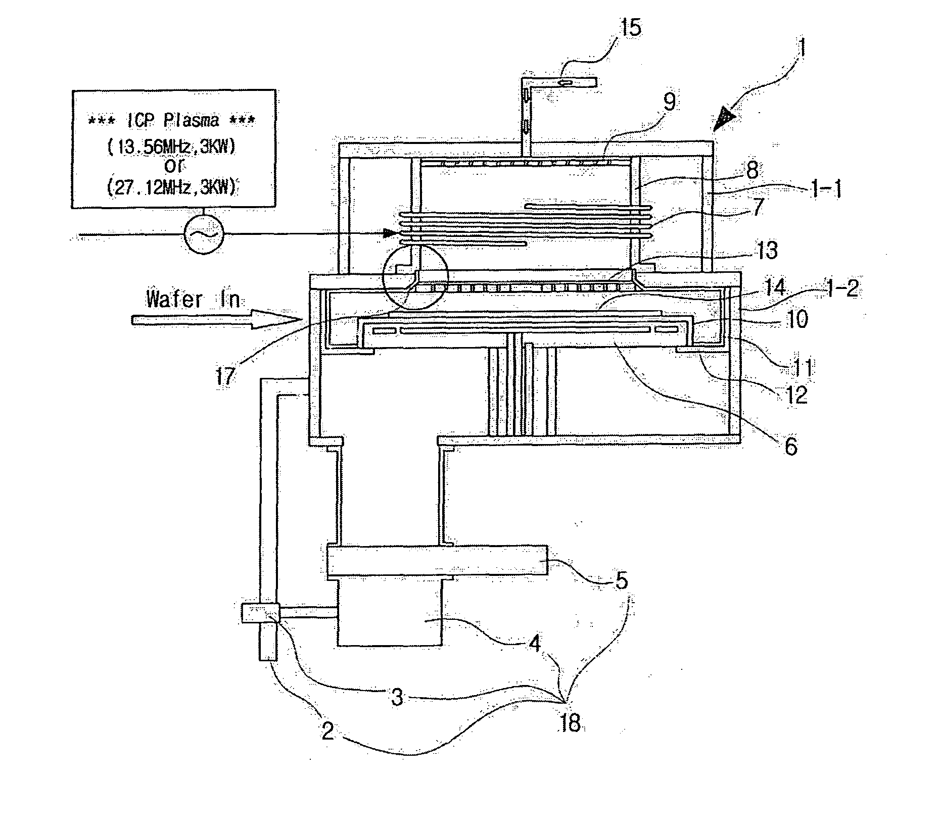
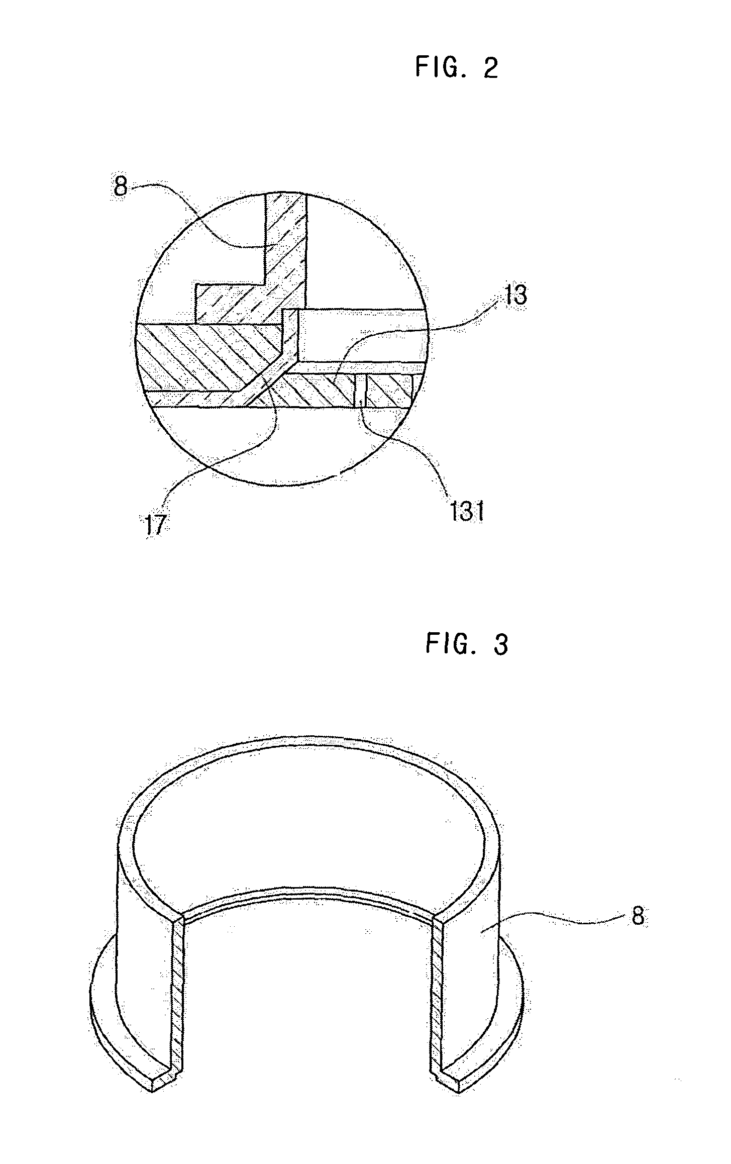
[0023]FIG. 1 is a schematic view showing an apparatus for surface-treating a wafer according to the present invention, FIG. 2 is a partially enlarged cross-sectional view showing the diffusion surface of a process chamber according to the present invention, FIG. 3 is a perspective view showing a cylinder according to the present invention, which is partly cut away, and FIG. 4 is a perspective view showing a gas distribution plate according to an embodiment of the present invention.

[0024]As shown in FIG. 1, the apparatus for surface-treating a wafer according to the present invention includes a process chamber 1 having a two-stage structure, which includes a plasma generation unit 1-1 located at the uppe...


PUM

PropertyMeasurementUnit
Temperatureaaaaaaaaaa
Pressureaaaaaaaaaa
Angleaaaaaaaaaa

Abstract

Disclosed herein is an apparatus for surface-treating a wafer using high-frequency inductively-coupled plasma, including a process chamber including a plasma generation unit into which a reaction gas is introduced and which generates plasma, and a wafer treatment unit in which any one or more selected from among plasma treatment, thin film formation and etching is performed; and a pressure control unit including a vacuum plate, and a pumping port, a two-stage valve, a turbo pump and an APC valve which are organically connected with the vacuum plate, to control a pressure in the process chamber and a pumping rate.

Description

TECHNICAL FIELD[0001]The present invention relates to a wafer surface treatment apparatus which can be used to plasma-treat a wafer, form a thin film on the wafer and then etch the thin film, using helical type high-frequency inductively-coupled plasma, and more particularly, to an apparatus for surface-treating a wafer using high-frequency inductively-coupled plasma, in which high-frequency inductively-coupled plasma (ICP) using a helical coil with four turns is employed, and thus the efficiency of plasma treatment is increased, in which a plasma source provided in a cylinder prevents plasma from being directly applied on the surface of a wafer, so that the deterioration of device characteristics of a work surface caused by plasma can be prevented, thereby maintaining effective process conditions for oxidation, nitridation, deposition, and etching, and which can prevent a wafer from sliding by embossing an upper surface of a heater cover.BACKGROUND ART[0002]Generally, when a coil i...

Claims


Application Information

Patent Timeline
IPC IPC(8): C23F1/08C23C16/00
CPCH01J37/3244H01J37/321
Inventor UM, PYUNG-YONG
Owner EUGENE TECH CO LTD
Why Eureka
Try Eureka