
ESD network circuit with a through wafer via structure and a method of manufacture

Active Publication Date: 2010-09-30
GLOBALFOUNDRIES US INC
View PDF24 Cites 16 Cited by
  • Summary
  • Abstract
  • Description
  • Claims
  • Application Information

AI Technical Summary

Benefits of technology

[0011]In a first aspect of the invention, an electrostatic discharge (ESD) structure, comprises an ESD active device and

Problems solved by technology

More specifically, noise isolation and the elimination of complementary metal-oxide semiconductor (CMOS) latchup are significant issues in advanced CMOS technology, radio frequency (RF) CMOS, and bipolar CMOS (BiCMOS) Silicon Germanium (SiGe) technology.
In CMOS I / O circuitry, undershoot and overshoot can lead to injection in the substrate, and simultaneous switching of circuitry where overshoot or undershoot injection occurs may lead to both noise injection and latchup conditions.
Also, supporting elements in these circuits, such as pass transistors, resistor elements, test functions, over voltage dielectric limiting circuitry, bleed resistors, keeper networks and other elements can be present, contributing to noise injection into the substrate and latchup.
Terrestrial emissions from radioactive events, such as alpha particles, and other radioactive decay emissions can also lead to latchup in semiconductors.

Method used


Image

  • ESD network circuit with a through wafer via structure and a method of manufacture
  • ESD network circuit with a through wafer via structure and a method of manufacture
  • ESD network circuit with a through wafer via structure and a method of manufacture

Examples


Embodiment Construction

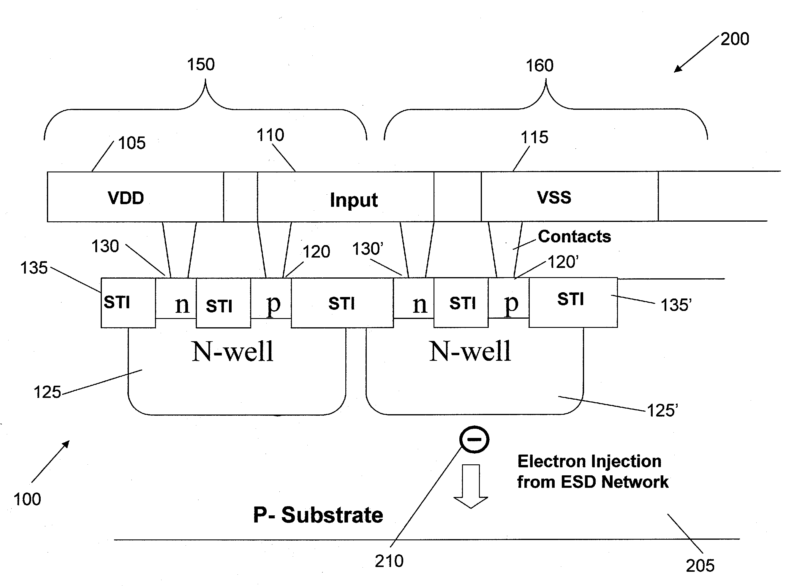
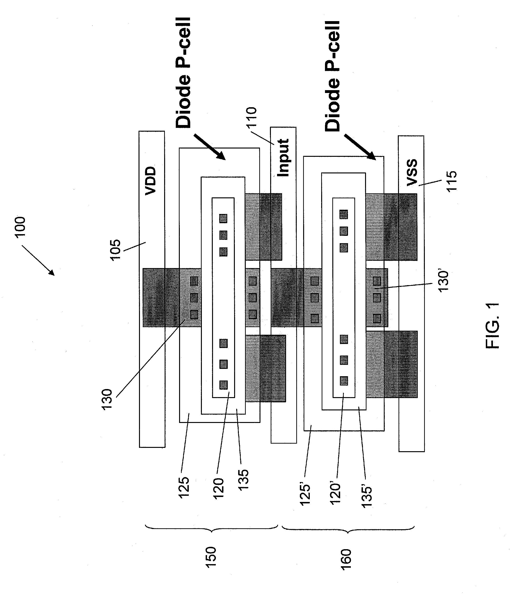
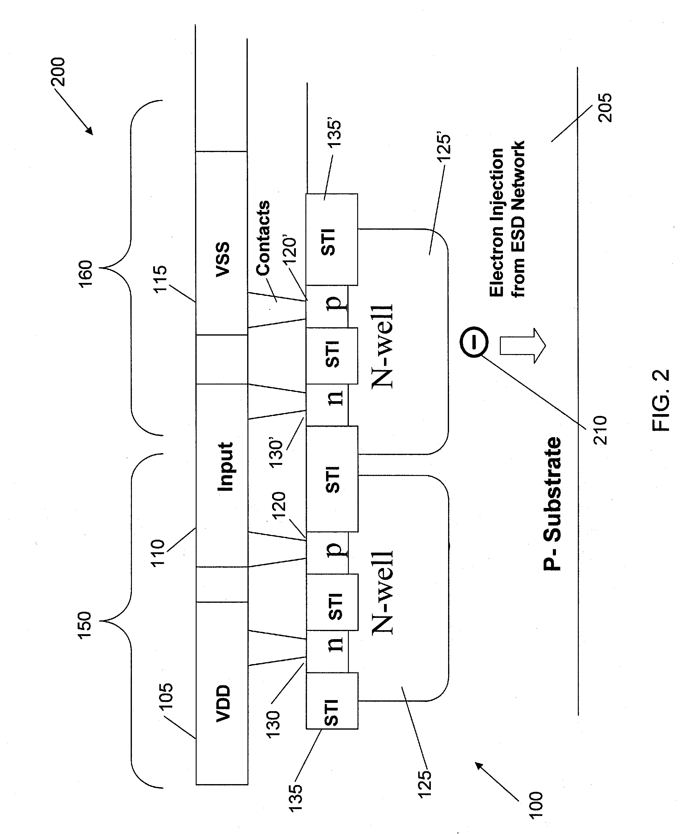
[0023]The present invention generally relates to a circuit structure and a method of manufacturing a circuit, and more specifically to an electrostatic discharge (ESD) circuit with a through wafer via structure and a method of manufacture. As discussed above, ESD circuits require low resistance shunt structures, which can, for example, dump current, power and / or heat. Additionally, as discussed above, ESD circuits utilize guard rings to isolate minority carrier injection to adjacent structures.

[0024]In accordance with aspects of the invention, a through wafer via may be used in an ESD structure to provide a low resistance path to the substrate for the ESD circuit. Additionally, the through wafer via can act as “guard ring” for the ESD circuit to prevent lateral minority carrier injection to adjacent structures and / or from injection sources, e.g., observed in NMOS, PMOS or CMOS semiconductor chips. By implementing the present invention, a through wafer via may be utilized to perform ...


PUM


Abstract

The present invention generally relates to a circuit structure and a method of manufacturing a circuit, and more specifically to an electrostatic discharge (ESD) circuit with a through wafer via structure and a method of manufacture. An ESD structure includes an ESD active device and at least one through wafer via structure providing a low series resistance path for the ESD active device to a substrate. An apparatus includes an input, at least one power rail and an ESD circuit electrically connected between the input and the at least one power rail, wherein the ESD circuit comprises at least one through wafer via structure providing a low series resistance path to a substrate. A method, includes forming an ESD active device on a substrate, forming a ground plane on a backside of the substrate and forming at least one through wafer via electrically connected to a negative power supply of the ESD active device and the ground plane to provide a low series resistance path to the substrate.

Description

FIELD OF THE INVENTION[0001]The present invention generally relates to a circuit structure and a method of manufacturing a circuit, and more specifically to an electrostatic discharge (ESD) circuit with a through wafer via structure and a method of manufacture.BACKGROUND OF THE INVENTION[0002]An ESD event refers to a phenomenon of electrical discharge of a current (positive or negative) for a short duration during which a large amount of current is provided to an integrated circuit (IC). The large current may be built-up from a variety of sources, such as the human body. An ESD event commonly results from the discharge of a high voltage potential (typically, several kilovolts) and leads to pulses of high current (several amperes) of a short duration (typically, 100 nanoseconds). An ESD event is generated within an IC, illustratively, by human contact with the leads of the IC or by electrically charged machinery being discharged in other leads of an IC. During installation of integra...

Claims


Application Information

Patent Timeline
IPC IPC(8): H01L29/861H01L21/02
CPCH01L23/481H01L23/5225H01L23/5227H01L23/585H01L23/60H01L25/0657H01L2924/0002H01L27/0248H01L2225/06541H01L2924/3011H01L2924/00
Inventor VOLDMAN, STEVEN H.
Owner GLOBALFOUNDRIES US INC
Features
  • Generate Ideas
  • Intellectual Property
  • Life Sciences
  • Materials
  • Tech Scout
  • Unparalleled Data Quality
  • Higher Quality Content
  • 60% Fewer Hallucinations
Learn More