Solid-state imaging device, signal processing method of solid-state imaging device, and electronic apparatus

a solid-state imaging and signal processing technology, applied in the direction of radioation controlled devices, television system scanning details, television systems, etc., can solve the problems of not increasing resolution, difficult to resolve a pixel pitch of 2 m or less, and difficult to resolve a pixel pitch of 5 m or less, so as to improve the imaging characteristic, improve the dynamic range, and improve the imaging characteristic

Active Publication Date: 2010-10-07
SONY CORP
View PDF13 Cites 23 Cited by
  • Summary
  • Abstract
  • Description
  • Claims
  • Application Information

AI Technical Summary

Benefits of technology

[0014]In the present invention, it is desirable to provide a solid-state imaging device, a signal processing method of a solid-state imaging device, and an electronic apparatus which perform calculation between adjacent pixels to provide an improved characteristic or a new function, to thereby achieve substantially the manageability of a square-pixel product and make image processing and system construction easier.
[0017]The plurality of rectangular pixels are combined to form a square pixel, and the plurality of signals read out from the plurality of rectangular pixels are output as a single signal. Thereby, the single signal can be handled as the signal from a square grid (a square pixel). If incident light is sampled at spatially equal intervals in the vertical and horizontal directions, it is possible to make the plurality of rectangular pixels look like a square grid. With the single signal handled as the signal from a square grid, it is unnecessary to change the configuration of a signal processing system for square grids at a subsequent stage. Further, if the single signal is selected as appropriate from or synthesized from the respective signals of the plurality of rectangular pixels, it is possible to perform a process of improving the imaging characteristic, such as a process of increasing the dynamic range by using the single signal in the signal processing system at the subsequent stage. As a result, even if the pixels are miniaturized beyond the limit of the resolution, it is possible to improve the imaging characteristic while realizing the miniaturization of the pixels.
[0018]According to the embodiment of the present invention, calculation is performed between adjacent pixels in the vertical or horizontal direction to provide an improved characteristic or a new function. Thereby, it is possible to achieve substantially the manageability of a square-pixel product, and to make image processing and system construction easier. It is also possible to improve the imaging characteristic, even if the pixels are miniaturized beyond the limit of the resolution, and if the pixel pitch becomes less than the resolution of an optical system which receives incident light.

Problems solved by technology

If the pixel pitch becomes less than the resolution of a lens, however, the resolution is not increased.
Even at F4, it is difficult to resolve the pixel pitch of 2 μm or less.
Therefore, it is difficult to resolve a pixel pitch of 5 μm or less.

Method used


Image

  • Solid-state imaging device, signal processing method of solid-state imaging device, and electronic apparatus
  • Solid-state imaging device, signal processing method of solid-state imaging device, and electronic apparatus
  • Solid-state imaging device, signal processing method of solid-state imaging device, and electronic apparatus

Examples


first embodiment

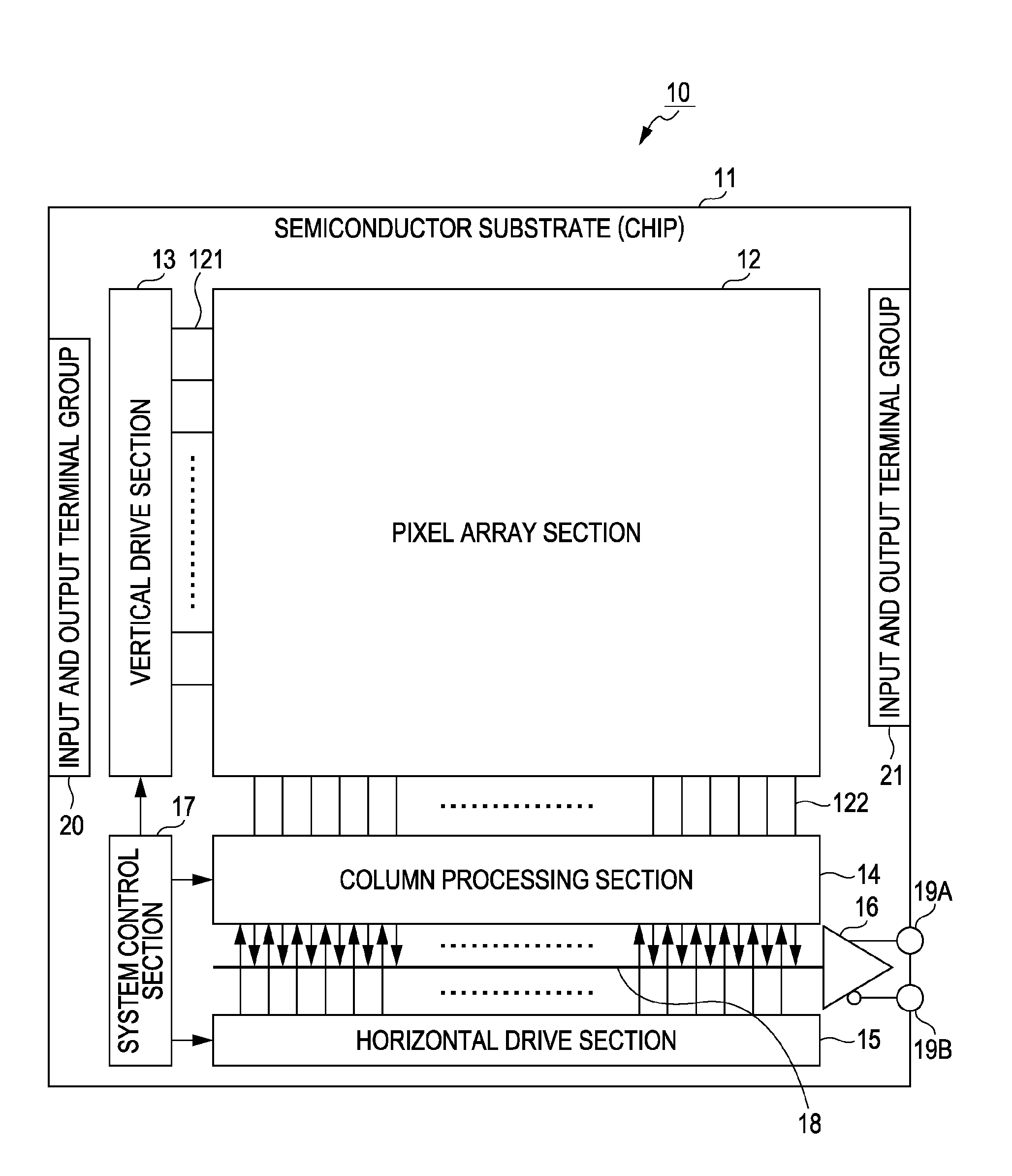
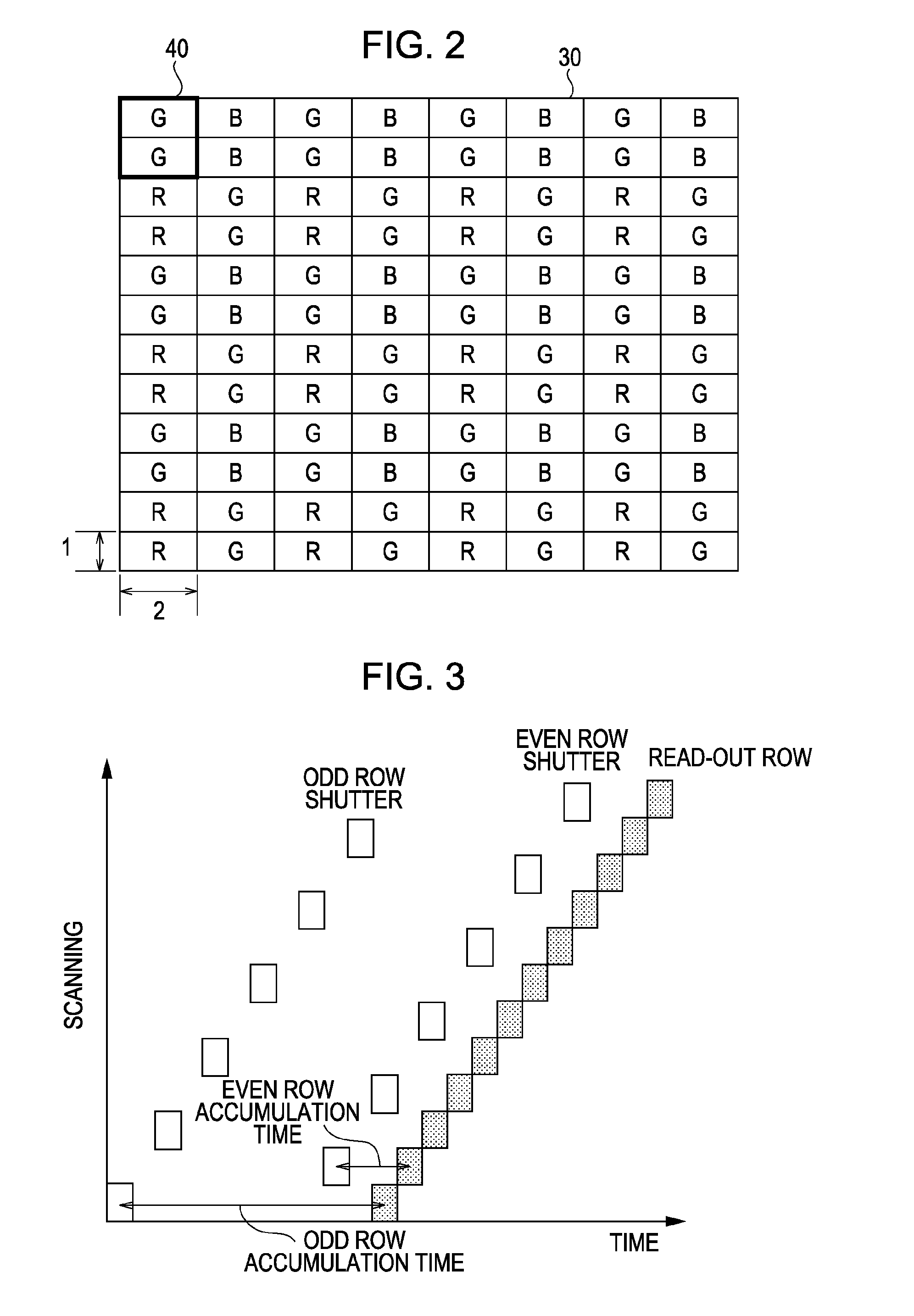
[0067]FIG. 2 is a configuration diagram illustrating an example of the pixel array in the pixel array section 12 according to a first embodiment. As illustrated in FIG. 2, the pixel array section 12 includes unit pixels 30 each including a photoelectric conversion element and two-dimensionally arranged in multiple rows and columns. Herein, each of the unit pixels 30 is a so-called horizontally long rectangular pixel, which is twice as long in the horizontal size (in the row direction) as in the vertical size (in the column direction), i.e., which has a vertical-to-horizontal pitch ratio of 1:2.

[0068]If the CMOS image sensor 10 according to the present embodiment is capable of picking up a color image, color filters, e.g., on-chip color filters 40, are provided on respective light receiving surfaces of the unit pixels 30. Herein, a plurality, e.g., two of the unit pixels 30 adjacent in the vertical direction form a set. The set of two upper and lower pixels is provided with an on-chi...

modified examples

[0177]In many CMOS image sensors, the individual on-chip color filter 40 is provided with on-chip lenses placed thereon for the respective pixels to improve the sensitivity. In the first embodiment, each of the unit pixels 30 has a horizontally long shape. Thus, it is difficult to precisely collect light by using the on-chip lenses. This is because it is difficult to produce a non-circular on-chip lens, and, in the first place, it is difficult to collect light by using a non-circular lens.

first modified example

[0178]To address the issue of collection of light by using the on-chip lenses, it is preferable to employ, as a back-surface incident type pixel structure or a photoelectric conversion film lamination type pixel structure, a pixel structure having an aperture ratio of 100% and not using the on-chip lenses. The back-surface incident type pixel structure receives incident light from the opposite side to a wiring layer. The photoelectric conversion film lamination type pixel structure performs photoelectric conversion at a photoelectric conversion film laminated on the incident light side of a wiring layer. An example of the back-surface incident type pixel structure will be described below.

[0179]FIG. 16 is a cross-sectional view illustrating an example of the back-surface incident type pixel structure. Herein, a cross-sectional structure of two pixels is illustrated.

[0180]In FIG. 16, photodiodes 42 and pixel transistors 43 are formed in a silicon portion 41. That is, the silicon porti...


PUM


Abstract

A solid-state imaging device includes a pixel array section and a signal processing section. The pixel array section is configured to include a plurality of arranged rectangular pixels, each of which has different sizes in the vertical and horizontal directions, and a plurality of adjacent ones of which are combined to form a square pixel having the same size in the vertical and horizontal directions. The signal processing section is configured to perform a process of outputting, as a single signal, a plurality of signals read out from the combined plurality of rectangular pixels.

Description

BACKGROUND OF THE INVENTION[0001]1. Field of the Invention[0002]The present invention relates to a solid-state imaging device, a signal processing method of a solid-state imaging device, and an electronic apparatus.[0003]2. Description of the Related Art[0004]In a solid-state imaging device, such as a CCD (Charge Coupled Device) image sensor and a CMOS (Complementary Metal-Oxide Semiconductor) image sensor, unit pixels are in many cases arranged in a grid-like pattern at a predetermined pitch in the vertical and horizontal directions (see Japanese Unexamined Patent Application Publication No. 2007-189085, for example).[0005]A pixel array having the same pitch in the vertical and horizontal directions is easily signal-processed, and thus has become a mainstream these days. Pixels arranged at the same pitch in the vertical and horizontal directions, i.e., pixels each having the same size in the vertical and horizontal directions are called square pixels. Meanwhile, pixels arranged at ...

Claims


Application Information

Patent Timeline
Patent Type & Authority Applications(United States)
IPC IPC(8): H04N5/335H04N5/228H01L27/146H04N5/355H04N5/369H04N5/374H04N5/378
CPCH01L27/14621H01L27/14625H01L27/14643H01L27/14641H04N5/35563H01L27/1464H04N5/23229H01L27/14627H01L27/14607H04N23/80H04N25/585H04N25/713H04N25/75H04N25/65H04N25/67H04N25/616H04N25/745H04N25/767
Inventor MABUCHI, KEIJI
Owner SONY CORP
Why Eureka
Try Eureka