

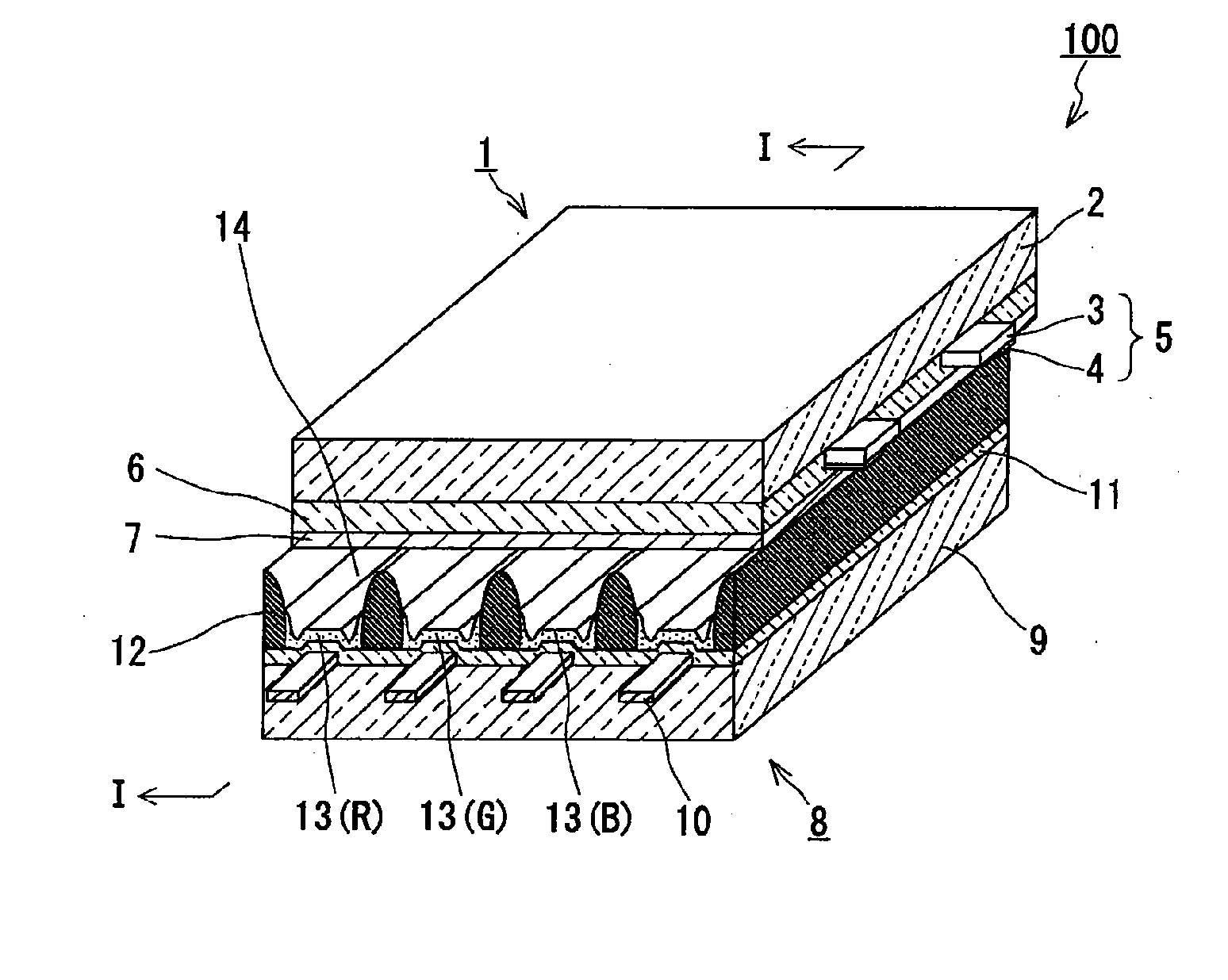
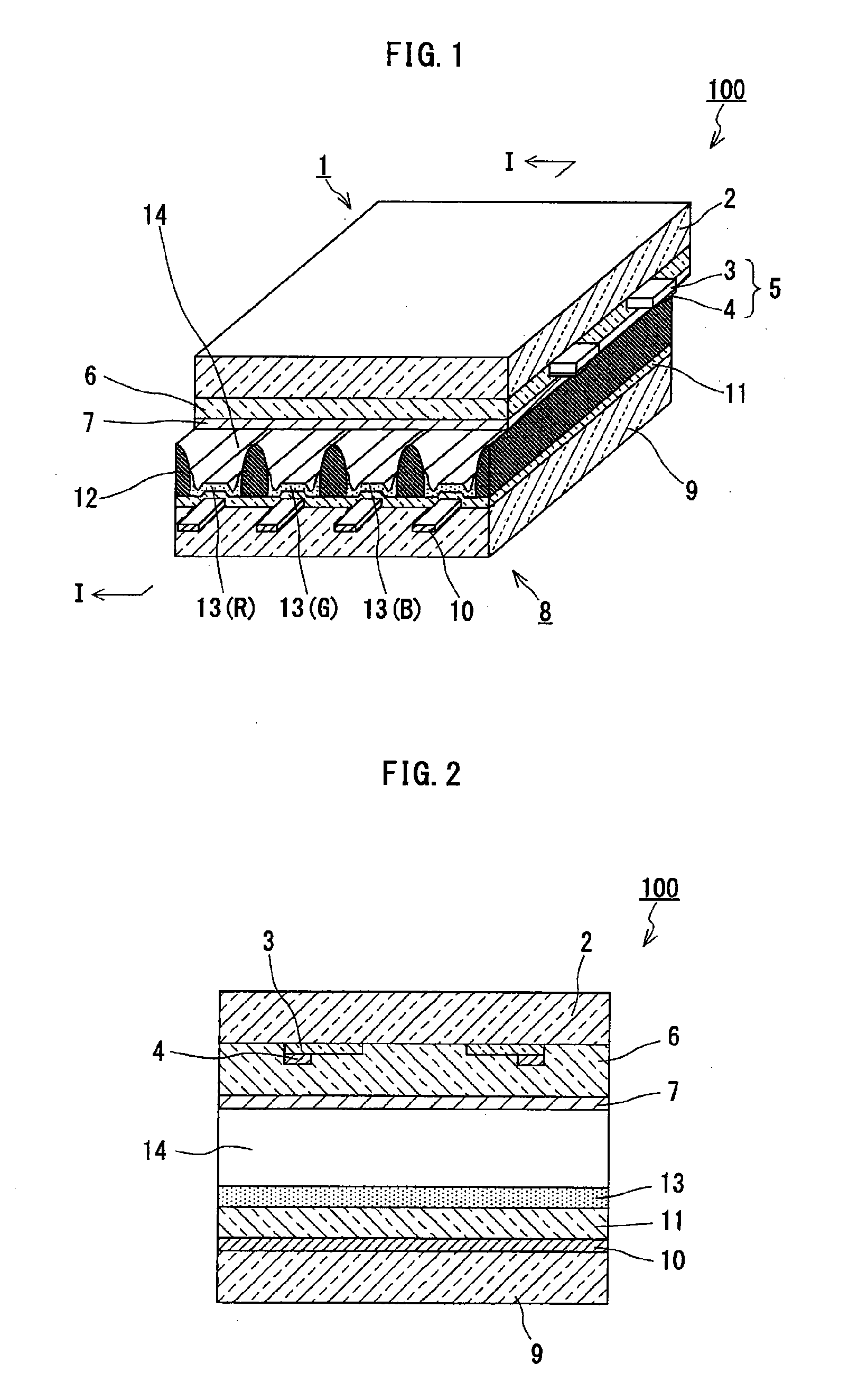
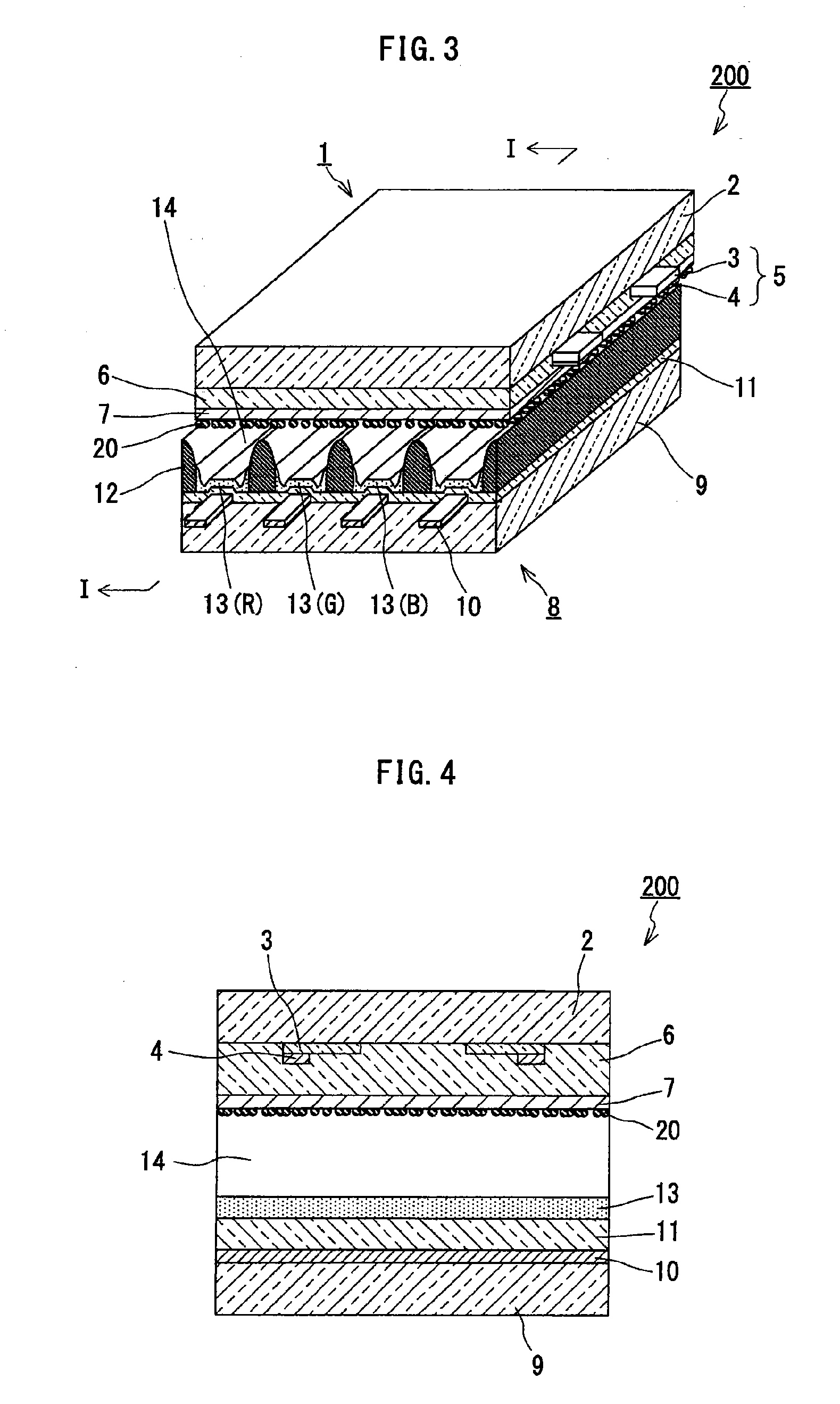
Plasma display panel
a technology of display panel and plasma, which is applied in the direction of electric discharge tubes, gas-filled discharge tubes, instruments, etc., can solve the problems of increasing the firing voltage and the sustaining voltage, and achieves the reduction of the drive voltage of the pdp, high secondary electron emission coefficient, and high resistance to ion bombardment
- Summary
- Abstract
- Description
- Claims
- Application Information
AI Technical Summary
Benefits of technology
Problems solved by technology
Method used
Image

Examples
embodiments
[0107]The following describes the present invention in more detail based on embodiments.
first embodiment
[0108]In this embodiment, an experiment was conducted to confirm an effect of improving chemical stability by reacting CaO, SrO and BaO with SnO2 by a solid phase powder method and synthesizing electron emissive materials (crystalline compounds).
[0109](Synthesis of Crystalline Compound)
[0110]Guaranteed reagent or purer CaCO3, SrCO3, BaCO3 and SnO2 were used as starting materials. After these materials are weighed so that a mole ratio of each metal ion shows each of No. 4 to 11 in Table 1, the weighed materials were wet blended with use of a ball mill, and dried out to obtain a mixed powder.
[0111]The obtained mixed powder was placed into a platinum crucible, and baked in the air at 1200 degrees Celcius to 1500 degrees Celcius for two hours in an electric furnace. After an average particle size of the baked mixed powder was measured, particles having particle sizes larger than the measured average particle size were wet milled using ethanol as a solvent. In this manner, the average pa...
second embodiment
[0171]In this embodiment, a case where composition rate of elements is changed, a case where solid solution with various metal oxides is formed, and a case where Ba or Sn is substituted with another metal are shown with a focus on BaSnO3.
[0172]In a similar manner to Embodiment 1, by using guaranteed reagent or purer CaCO3, SrCO3, BaCO3, SnO2 and various metal oxides as starting materials, the inventors weighed these materials so that element ratios show composition ratios (atom ratios) shown in Table 4, and mixed, dried out and baked the weighed materials to synthesize powders of compounds shown in Table 4.
[0173]Identification by an X-ray diffraction, evaluation of hygroscopicity, and XPS measurement were performed for the synthesized compounds. Furthermore, similarly to Embodiment 1, PDPs were produced by using apart of these powders, and discharge voltage of these PDPs was measured. At this time, although discharge voltage was measured after PDPs were aged by holding the PDPs for ...
PUM
 Abstract
Description
Claims
Application Information