Semiconductor memory device and data processing device

Inactive Publication Date: 2010-10-21
SEMICON ENERGY LAB CO LTD
View PDF22 Cites 15 Cited by
  • Summary
  • Abstract
  • Description
  • Claims
  • Application Information

AI Technical Summary

Benefits of technology

[0023]By the above-described semiconductor memory device, an operation time of the boosting circuit can be optimized. Thus, unnecessary current consumption which is caused by an operation of the boosting circuit after the memory element is shorted can be suppressed. In addition, at the same time as the boosting circuit stops an operation, a writing operation finishes, whereby a writing time can be optimized. In addition to those effects, the following can be

Problems solved by technology

A problem in an antifuse memory is that a period of time needed for transition from an insulating state to a shorted state, that is, a writing time, varies considerably between memory cells.
Typically, although writing into most of the memory cells finish in a short time, writing into a small number of memory cells needs a longer time.
In addition, the period may cause an adverse effect du

Method used


Image

  • Semiconductor memory device and data processing device
  • Semiconductor memory device and data processing device
  • Semiconductor memory device and data processing device

Examples


embodiment 1

[0048]In Embodiment 1, an example of a structure of a semiconductor memory device will be described with reference to a drawing.

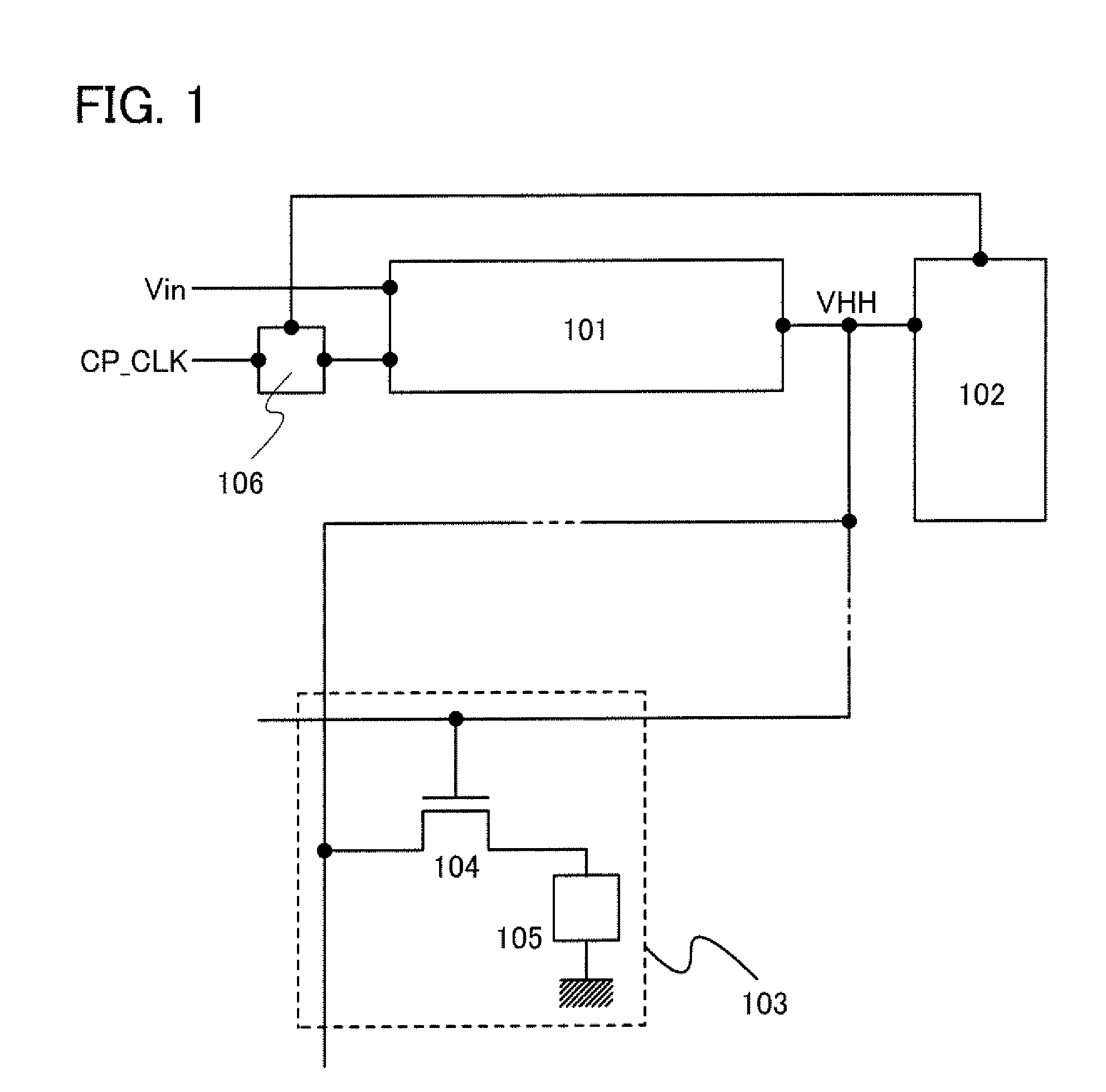
[0049]FIG. 1 is a block diagram of one example of a memory module on which an OTP memory is mounted. The memory module in FIG. 1 has a function of feeding back a change in output voltage of a boosting circuit in writing to a signal input to the boosting circuit. In the block diagram in FIG. 1, a boosting circuit 101, a monitor circuit 102, a memory cell 103, and a control circuit 106 are shown. The memory cell 103 includes a transistor 104 and a memory element 105. Although not shown, a capacitor may be connected in parallel to the memory element 105 in order to improve a writing yield.

[0050]In a writing operation, the boosting circuit 101 boosts an input voltage (Vin) using a clock signal (CP_CLK) and outputs the boosted voltage as an output voltage (VHH). The output voltage (VHH) of the boosting circuit 101 is applied to the memory element 105 through the...

embodiment 2

[0054]In Embodiment 2, a more specific structure of a semiconductor memory device will be described with reference to drawings.

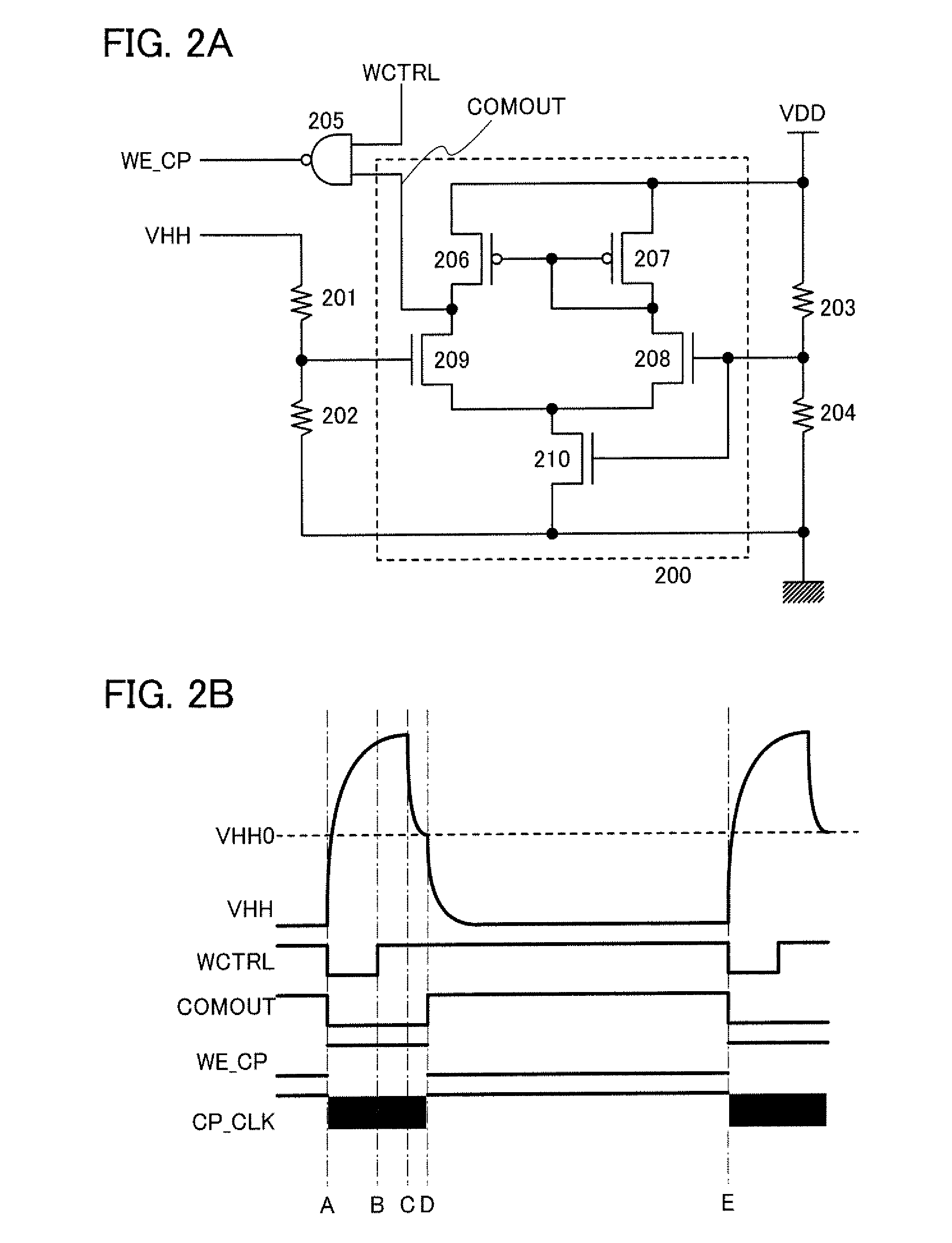
[0055]FIG. 2A is a circuit diagram showing an example of a monitor circuit mounted on the memory module described in Embodiment 1. The circuit in FIG. 2A includes a comparator 200, resistors 201 and 202 for dividing the output voltage (VHH) of the boosting circuit to be input to the comparator 200, resistors 203 and 204 for dividing a power supply voltage (VDD) to be input to the comparator 200 for comparison with the output voltage (VHH) of the boosting circuit, and a NAND gate 205 which outputs the logical NAND of an output (COMOUT) of the comparator 200 and a writing control signal (WCTRL). The comparator 200 includes transistors 206 to 210.

[0056]The comparator 200 compares voltages applied to two input terminals (here, a gate electrode of the transistor 208 and a gate electrode of the transistor 209). When one of the voltages is higher than the other, th...

embodiment 3

[0071]In Embodiment 3, a more specific structure of a semiconductor memory device according to one embodiment of the present invention will be described with reference to drawings.

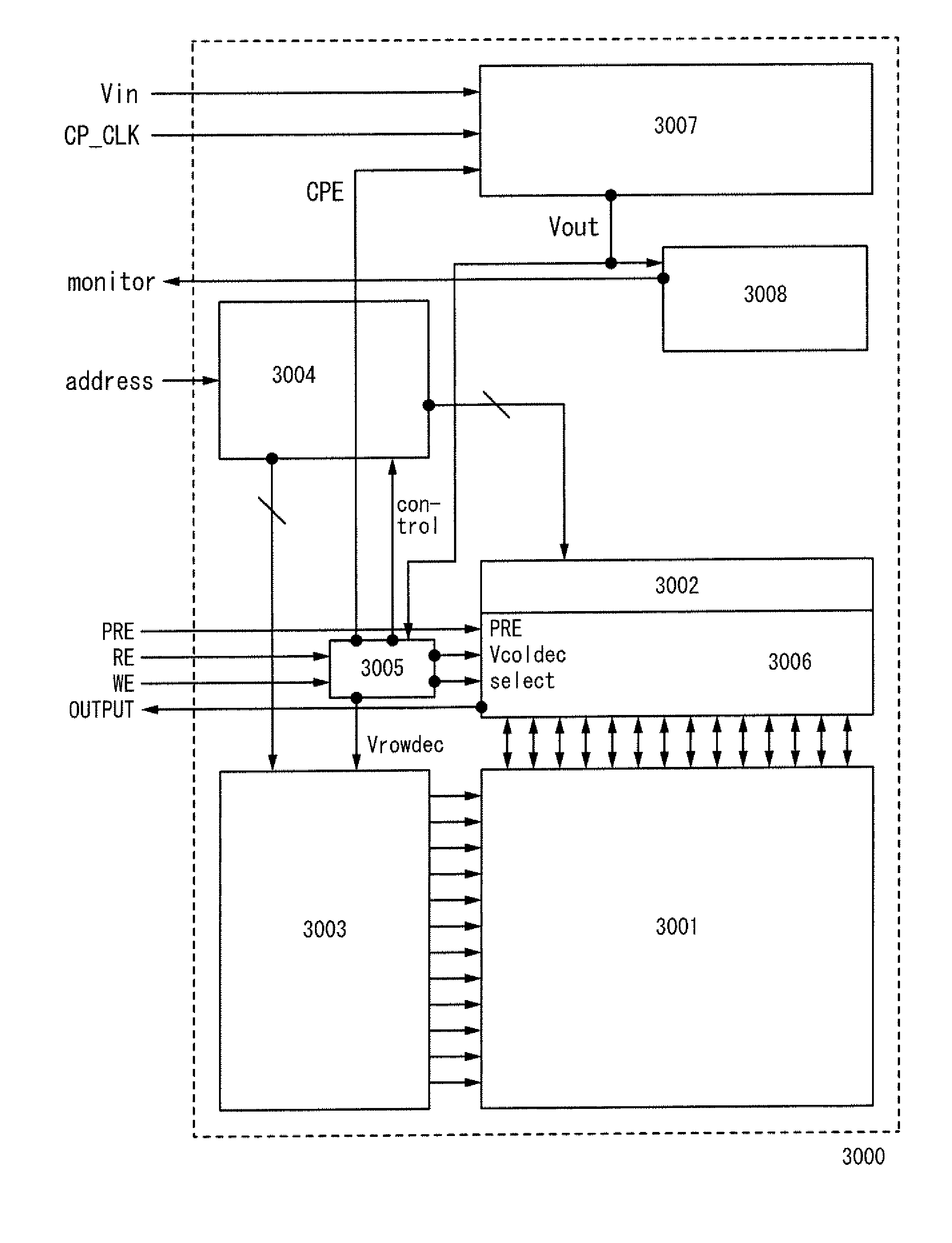
[0072]FIG. 6 is a block diagram of an example of a memory circuit in which memory cells and circuits necessary for driving the memory cells are modularized. As illustrated in FIG. 6, a memory circuit 3000 includes a memory cell array 3001, a column decoder 3002, a row decoder 3003, an address selector 3004, a selector 3005, a reading / writing circuit 3006, a boosting circuit 3007, and a monitor circuit 3008. Here, the memory cell array 3001 includes a plurality of memory cells arranged in a matrix.

[0073]Next, the operation of the memory circuit 3000 will be described. To the memory circuit 3000, a read enable signal (RE), a write enable signal (WE), an address signal (address), and a clock signal (CP_CLK) which is supplied to the boosting circuit are input as operation signals, and the input voltage (Vin) f...


PUM


Abstract

When writing into an antifuse memory element finishes, a value of resistance of the memory element rapidly decreases; accordingly, an output voltage of a boosting circuit which produces a writing voltage rapidly decreases. By detecting a change in the output voltage of the boosting circuit to control a writing command, the writing operation can be stopped immediately after the memory element is shorted. Thus, unnecessary current consumption caused by continuing a writing operation on the shorted memory element can be suppressed.

Description

BACKGROUND OF THE INVENTION[0001]1. Field of the Invention[0002]The present invention relates to semiconductor memory devices. Further, the present invention relates to semiconductor devices on which semiconductor memory devices are mounted.[0003]2. Description of the Related Art[0004]Recently, an individual-recognition technology has attracted attention. In the individual-recognition technology, an individual identification number (ID) is given to each individual object so that information such as a history of the object can be identified and used for production, management, and the like. In particular, an individual-recognition technology in which semiconductor devices which are capable of transmitting and receiving data without contact are used has been developed and starts to be introduced into companies, markets, and the like. Such a semiconductor device is referred to as a radio frequency identification (RFID) tag, an RF tag, an ID tag, an integrated circuit (IC) tag, an IC ch...

Claims


Application Information

Patent Timeline
IPC IPC(8): G11C17/00G11C5/14
CPCG11C5/145H01L27/101H01L23/5252G11C17/18H01L2924/0002H01L2924/00
Inventor SAITO, TOSHIHIKO
Owner SEMICON ENERGY LAB CO LTD
Why Eureka
Try Eureka