Surface emitting laser module and vertical illuminated photodiode module

a laser module and laser module technology, applied in the field of optical modules, can solve the problems of reducing the height the limitation of reducing the cost of the entire package, and the limitation of reducing the man-day for manufacture, etc., and achieves the effect of highly efficient optical coupling, highly dense packaging, and convenient self-alignmen

Inactive Publication Date: 2010-10-21
HITACHI LTD
View PDF7 Cites 29 Cited by
  • Summary
  • Abstract
  • Description
  • Claims
  • Application Information

AI Technical Summary

Benefits of technology

[0018]Owing to the employment of a light emitting diode or light receiving diode having a retaining section, which retains an external optical waveguide (optical fiber), integrated thereinto, the optical fiber and light emitting diode or the like can be readily self-aligned. In additi...

Problems solved by technology

Therefore, there are limitations in reducing the cost of the entire package and decreasing the height of the entire package.
Eventually, high-density packaging is confronted wit...

Method used


Image

  • Surface emitting laser module and vertical illuminated photodiode module
  • Surface emitting laser module and vertical illuminated photodiode module
  • Surface emitting laser module and vertical illuminated photodiode module

Examples


first embodiment

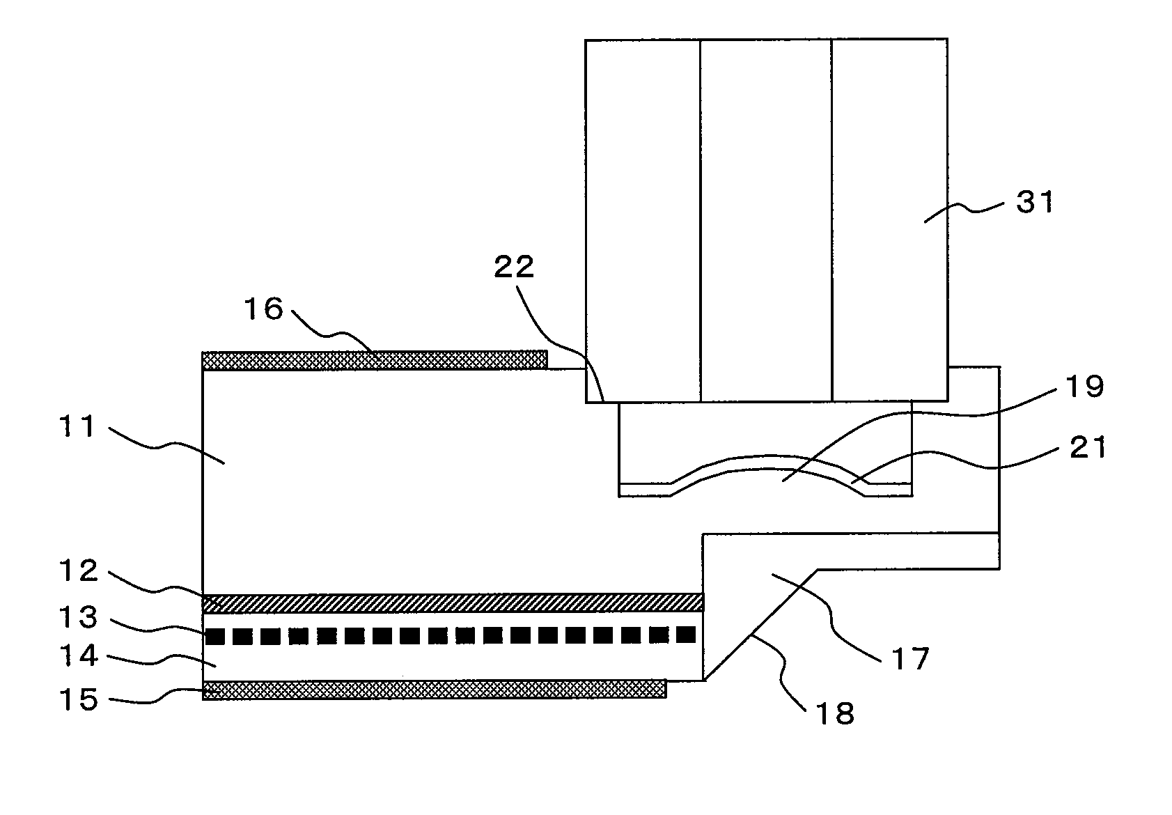
[0040]The construction of an optical module in accordance with a first embodiment will be described in conjunction with FIG. 1A, FIG. 1B, and FIG. 6. The present embodiment is an example in which a horizontal cavity vertical emission laser diode (third type) is adopted as a light emitting diode.

[0041]FIG. 1A is a sectional view of a plane horizontal to a cavity of a laser diode, and FIG. 1B shows a light emitting surface of the laser diode. The horizontal cavity vertical emission laser diode employed in the present embodiment has an active layer 12 layered or grown on an n-type semiconductor substrate 11. A grating layer 13, a p-type cladding layer 14, and a p-type electrode 15 are formed on the active layer 12. Nitrogen-doped indium phosphide (InP) is used to form the n-type semiconductor substrate 11, and a strained quantum well structure made of indium gallium aluminum arsenide (InGaAlAs) is adopted for the active layer 12. Gallium indium arsenide phosphide (GaInAsP) or the like ...

second embodiment

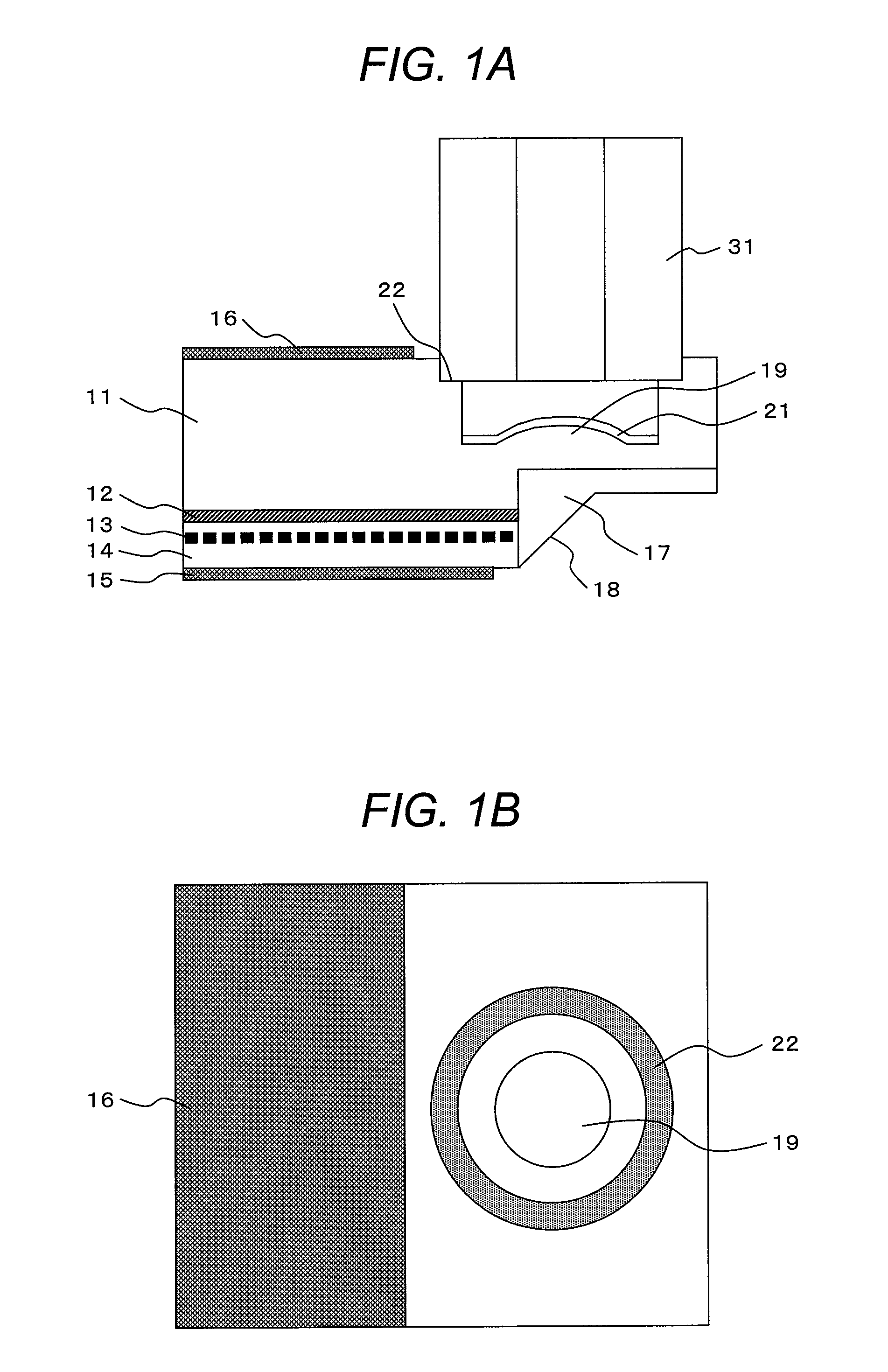
[0071]Referring to FIG. 2A and FIG. 2B, a second embodiment employing another horizontal cavity vertical emission laser diode will be described below. The components that have been described in relation to the first embodiment but will not be described in relation to the present embodiment are identical to those of the first embodiment.

[0072]FIG. 2A is a sectional view of a plane of a laser diode, which is employed in an optical module in accordance with the present embodiment, horizontal to a cavity. FIG. 2B shows a light emitting surface of the laser diode. In the present embodiment, a dent is formed in an n-type semiconductor substrate 11, and an integrated lens 19 is, similarly to the one of the first embodiment, formed on the bottom of the dent by etching the n-type semiconductor substrate 11. The lens 19 may be formed using any other material integrated into the substrate 11. Any other material may be processed to form the lens 19, and the lens 19 may then be integrated into t...

third embodiment

[0077]Referring to FIG. 3, a third embodiment employing another horizontal cavity vertical emission laser diode will be described below. The components that have been described in relation to the first or second embodiment but will not be described in relation to the present embodiment are identical to those of the first or second embodiment.

[0078]FIG. 3 is a sectional view of a plane of a laser diode, which is employed in an optical module in accordance with the present embodiment, horizontal to a cavity. Similarly to the second embodiment, a concave step formation integrated member 23b is integrated into the n-type semiconductor substrate 11. Unlike the second embodiment, a dent in an optical fiber retaining section (concave step) 24b is, as shown in FIG. 3, formed to have a slope. The slope is designed to square with an angle of the slope of an anti-reflection obliquely cut optical fiber. The dent is tilted at approximately 8° with respect to a horizontal plane. Therefore, when t...


PUM


Abstract

In order to provide a compact optical module permitting highly efficient optical coupling and having components thereof highly densely packaged, a light emitting diode that is included in the optical module and emits light in a vertical direction with respect to a principal surface of a semiconductor substrate is provided with a lens integrated into a light emitting region, and a retaining section integrated to surround the light emitting region. Accordingly, readiness in alignment of the light emitting diode and an optical fiber, which guides light emitted from the light emitting diode, with each other is upgraded. Eventually, the compact optical module permitting highly efficient optical coupling and having components thereof highly densely packaged can be provided.

Description

CLAIM OF PRIORITY[0001]The present application claims priority from Japanese patent application JP 2009-101963 filed on Apr. 20, 2009, the content of which is hereby incorporated by reference into this application.BACKGROUND OF THE INVENTION[0002]1. Field of the Invention[0003]The present invention relates to an optical module, or more particularly, to an optical module having a surface emitting laser diode or a vertically illuminated photodiode packaged, such as an optical transmission module or a CAN module.[0004]2. Description of the Related Art[0005]In recent years, in the field of information and telecommunications, data communication networks over which a large amount of data is transferred at a high speed using light have been rapidly brought into service, and optical fiber networks such as a backbone network, access networks, and metropolitan area networks have been deployed over the relatively long distances of several kilometers or more. In the future, it will prove effect...

Claims


Application Information

Patent Timeline
IPC IPC(8): H01S5/026H01S5/20H01S5/18H01L31/0232
CPCG02B6/322G02B6/4214G02B6/423H01S5/0207H01S5/18311H01S5/02284H01S5/0267H01S5/12H01S5/18H01S5/02212H01S5/02251
Inventor ADACHI, KOICHIROMATSUOKA, YASUNOBUSUGAWARA, TOSHIKIAOKI, MASAHIRO
Owner HITACHI LTD
Why Eureka
Try Eureka