Laminated structure for cis based solar cell, and integrated structure and manufacturing method for cis based thin-film solar cell

a technology of cis and solar cells, which is applied in the manufacture of final products, basic electric elements, climate sustainability, etc., can solve the problems of high waste treatment cost and a manufacturing cost of cis solar cells, and the film-forming of stable reactions at a certain point may not be performed, and achieves high production efficiency and buffer layer high resistance

Inactive Publication Date: 2010-10-21
SOLAR FRONTIER
View PDF10 Cites 74 Cited by
  • Summary
  • Abstract
  • Description
  • Claims
  • Application Information

AI Technical Summary

Benefits of technology

[0047]According to the present invention, since entire production lines can be carried out by a dry treatment process, the high-resistance buffer layer can be formed efficiently and stably.
[0048]Also, since the high-resistance buffer layer can be formed without using the solution growth method, the waste treatment plant for detoxifying ammonia required at the time of film-formation by the solution growth method as in the conventional case is not required and the production efficiency becomes high, so that the production cost can be reduced.
[0049]Also, the process in the larger area is possible and the film-forming rate is dramatically higher as compared to the ALD method, which is another dry manufacturing method, so that the productivity can be improved.
[0050]Also, according to the laminated structure of the present invention, the power collecting resistance loss can be reduced.

Problems solved by technology

However, in the conventional invention disclosed in Patent Document 1, although the effort has been made to minimize wastes containing Cd having high toxicity when allowing the cadmium sulfide (CdS) layer to grow as the high-resistance buffer layer, since solid CdS and alkaline wastes are generated in large volume, there has been a problem that a waste treatment cost becomes higher and a manufacturing cost of the CIS solar cell becomes higher.
In this case also, mixture of solid ZnO / ZnS and alkaline wastes are generated in large volume, so that there has been a problem that the waste treatment cost makes the manufacturing cost of the solar cell high.
Also, since the chemical bath deposition method is nonequilibrium chemical reaction, there has been a problem that film-formation by stable reaction at a certain point may not be performed.
Also, there has been a problem in production that the more the production scale increases, the larger the waste plant required for detoxifying ammonia used for maintaining alkaline property of the solution.
Also, since in-line manufacturing is not possible in the chemical bath deposition method, there has been a problem that production efficiency deteriorates.

Method used


Image

  • Laminated structure for cis based solar cell, and integrated structure and manufacturing method for cis based thin-film solar cell
  • Laminated structure for cis based solar cell, and integrated structure and manufacturing method for cis based thin-film solar cell
  • Laminated structure for cis based solar cell, and integrated structure and manufacturing method for cis based thin-film solar cell

Examples


Embodiment Construction

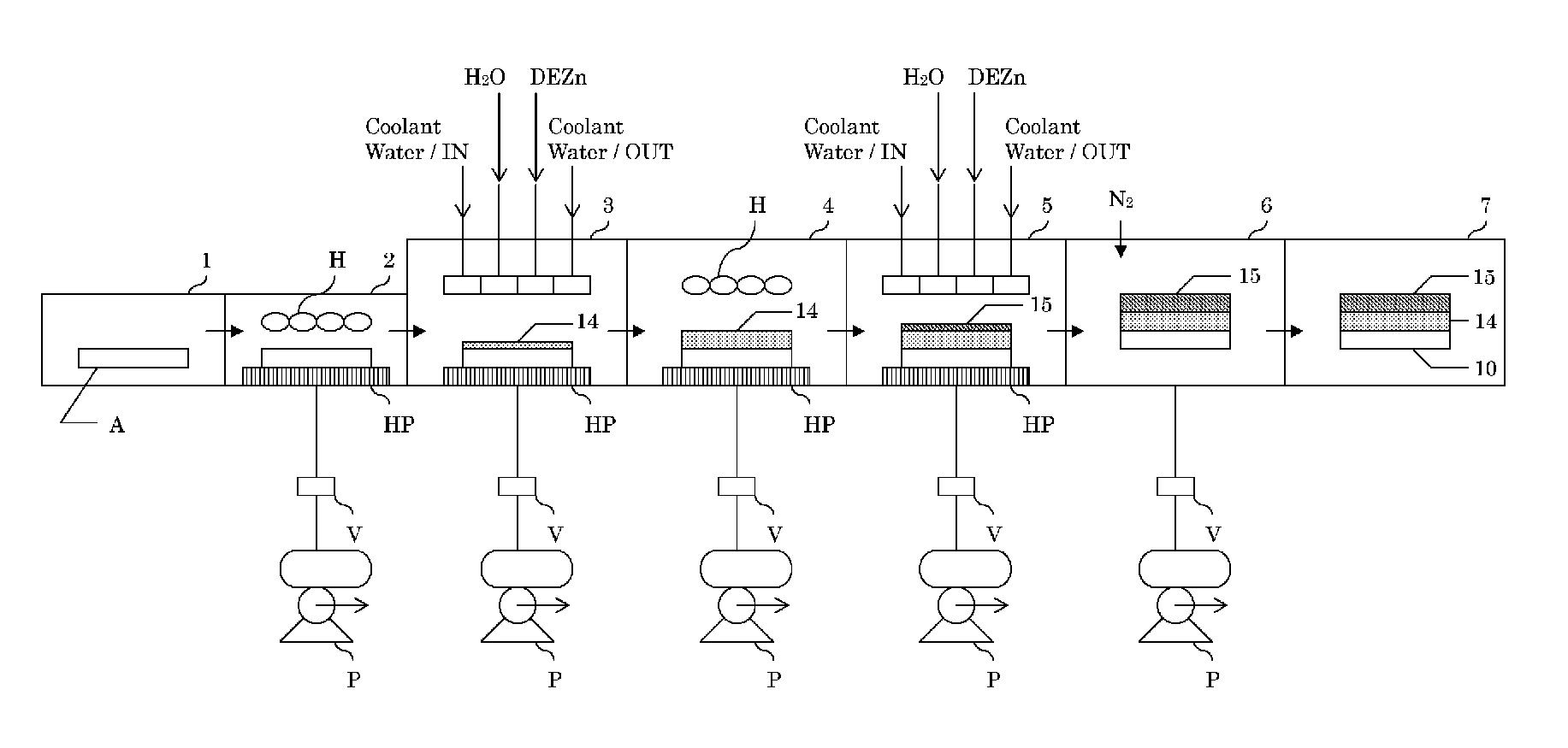
[0080]A laminated structure of a CIS based thin-film solar cell according to this embodiment will be described.

[0081]As illustrated in FIG. 1(a), a CIS based thin-film solar cell 1 according to this embodiment forms a p-n heterojunction device having a substrate structure obtained by laminating a glass substrate 11, a metal back electrode layer 12, a p-type CIS based light absorbing layer (hereinafter, simply referred to as an “light absorbing layer”) 13, a high-resistance buffer layer 14, an n-type window layer (transparent conductive film (hereinafter, simply referred to as a “window layer”)) 15 in this order.

[0082]The glass substrate 11 is a substrate on which the above-described layers are laminated, and a glass substrate such as soda-lime glass, a metal substrate such as a stainless plate and a resin substrate such as a polyimide film are used.

[0083]The metal back electrode layer 12 is highly corrosion-resistant metal such as Mo or Ti having a high melting point and a thickness...


PUM


Abstract

This invention aims to provide a laminated structure and an integrated structure of a high production efficiency for a CIS based thin-film solar cell, which can produce a high-resistance buffer layer of the CIS based thin-film solar cell efficiently on a series of production lines and which needs no treatment of wastes or the like, and a manufacturing method for the structures. The CIS based thin-film solar cell includes a back electrode, a p-type CIS based light absorbing layer, a high-resistance buffer layer and an n-type transparent conductive film laminated in this order. The high-resistance buffer layer and the n-type transparent conductive film are formed of thin films of a zinc oxide group. The buffer layer contacts the p-type CIS based light absorbing layer directly, and has a resistivity of 500 Ω·cm or higher.

Description

TECHNICAL FIELD[0001]The present invention relates to a laminated structure of a CIS based thin-film solar cell and a method for manufacturing the CIS based solar cell.BACKGROUND ART[0002]Currently, the CIS based thin-film solar cell is widely and practically used. When manufacturing the CIS based solar cell, it is assumed that the thin-film solar cell having high conversion efficiency may be obtained by allowing a cadmium sulfide (CdS) layer to grow as a high-resistance buffer layer on a light absorbing layer formed of a CuInSe2 thin film. Patent Document 1 discloses that, in a chemical bath deposition method for chemically forming a CdS thin film from solution, by immersing the CuInSe2 thin-film light absorbing layer in the solution, high-quality heterojunction with the thin-film light absorbing layer is formed and there is an effect to increase shunt resistance.[0003]Also, Patent Document 2 discloses the manufacturing method capable of obtaining the thin-film solar cell having hi...

Claims


Application Information

Patent Timeline
Patent Type & Authority Applications(United States)
IPC IPC(8): H01L31/18
CPCH01L31/0296Y02E10/541H01L31/1836H01L31/0749Y02P70/50
Inventor HAKUMA, HIDEKITABUCHI, KATSUYAFUJIWARA, YOSUKEKUSHIYA, KATSUMI
Owner SOLAR FRONTIER
Why Eureka
Try Eureka