

Atomic layer deposition of hafnium lanthanum oxides
a technology of hafnium lanthanum oxide and atomic layer, which is applied in the direction of semiconductor devices, semiconductor/solid-state device details, electrical equipment, etc., can solve the problems of increasing leakage current, unsatisfactory effects, and controlling leakage current to maintain high speed and low power performan
- Summary
- Abstract
- Description
- Claims
- Application Information
AI Technical Summary
Benefits of technology
Problems solved by technology
Method used
Image

Examples
Embodiment Construction
[0001]1. Field of the Invention
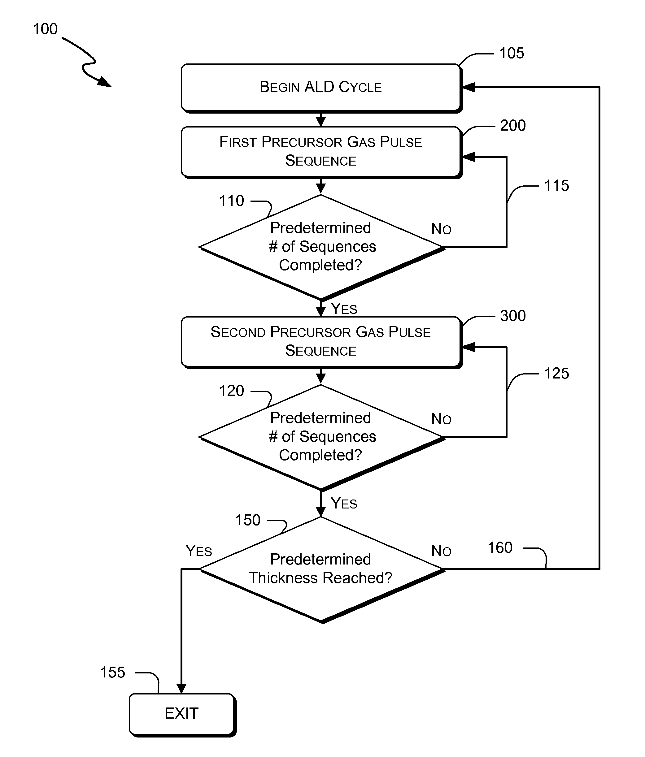
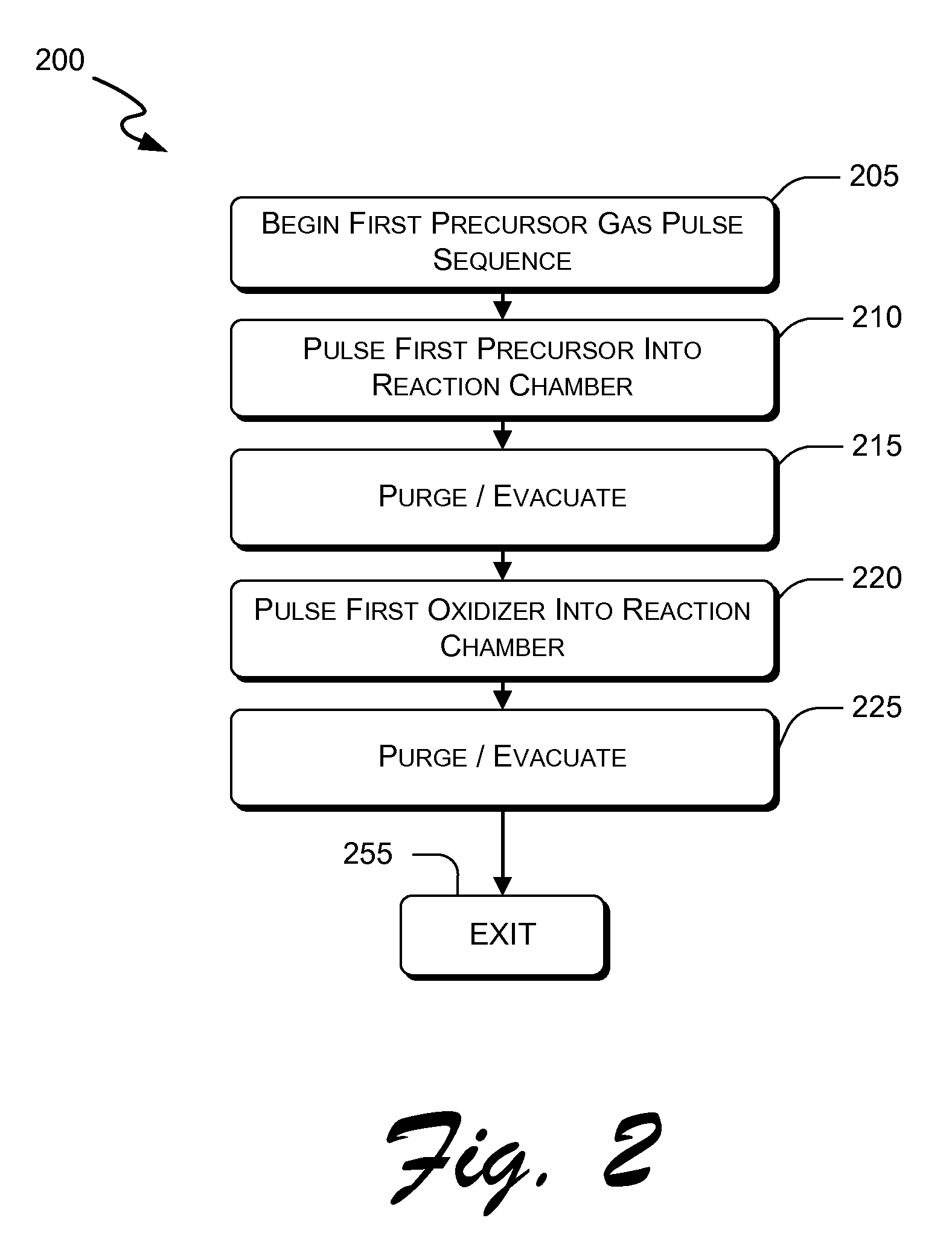
[0002]The present invention relates to thin film deposition, and more particularly methods using precursors to deposit hafnium lanthanum oxides by atomic layer deposition and components incorporating hafnium lanthanum oxide dielectric layers formed by methods consistent with the invention.
[0003]2. Background of the Invention
[0004]For many years, silicon dioxide (SiO2) has been used in semiconductor substrates for components such as transistor gate dielectrics and capacitor dielectrics. However, as circuit components have reduced in size, the electrical performance characteristics of SiO2 result in undesirable effects such as increased leakage current. Controlling leakage current to maintain high speed and low power performance presents a challenge when older-generation dielectrics such as SiO2 are used in the fabrication of newer integrated circuit geometries.
[0005]Newer processes, especially those that use fabrication geometries less than 65 nm have b...
PUM
 Abstract
Description
Claims
Application Information