
Photonic crystal element

a technology crystal elements, applied in the field of photonic crystal elements, can solve the problems of resonator stubs not being used, specific frequency bands not being able to propagate within the photonic crystal, and increasing manufacturing costs

Inactive Publication Date: 2010-11-04
NEC CORP
View PDF3 Cites 24 Cited by
  • Summary
  • Abstract
  • Description
  • Claims
  • Application Information

AI Technical Summary

Benefits of technology

The present invention provides a structure of a waveguide that has a narrow-band filter characteristic for lights having multiple wavelengths in a transmission band. This is achieved by using a photonic crystal with a waveguide within it that can guide a light within a specific frequency range. A waveguide stub is also connected to control the light within the waveguide. This results in a waveguide that can filter out specific lights within a certain range of wavelengths.

Problems solved by technology

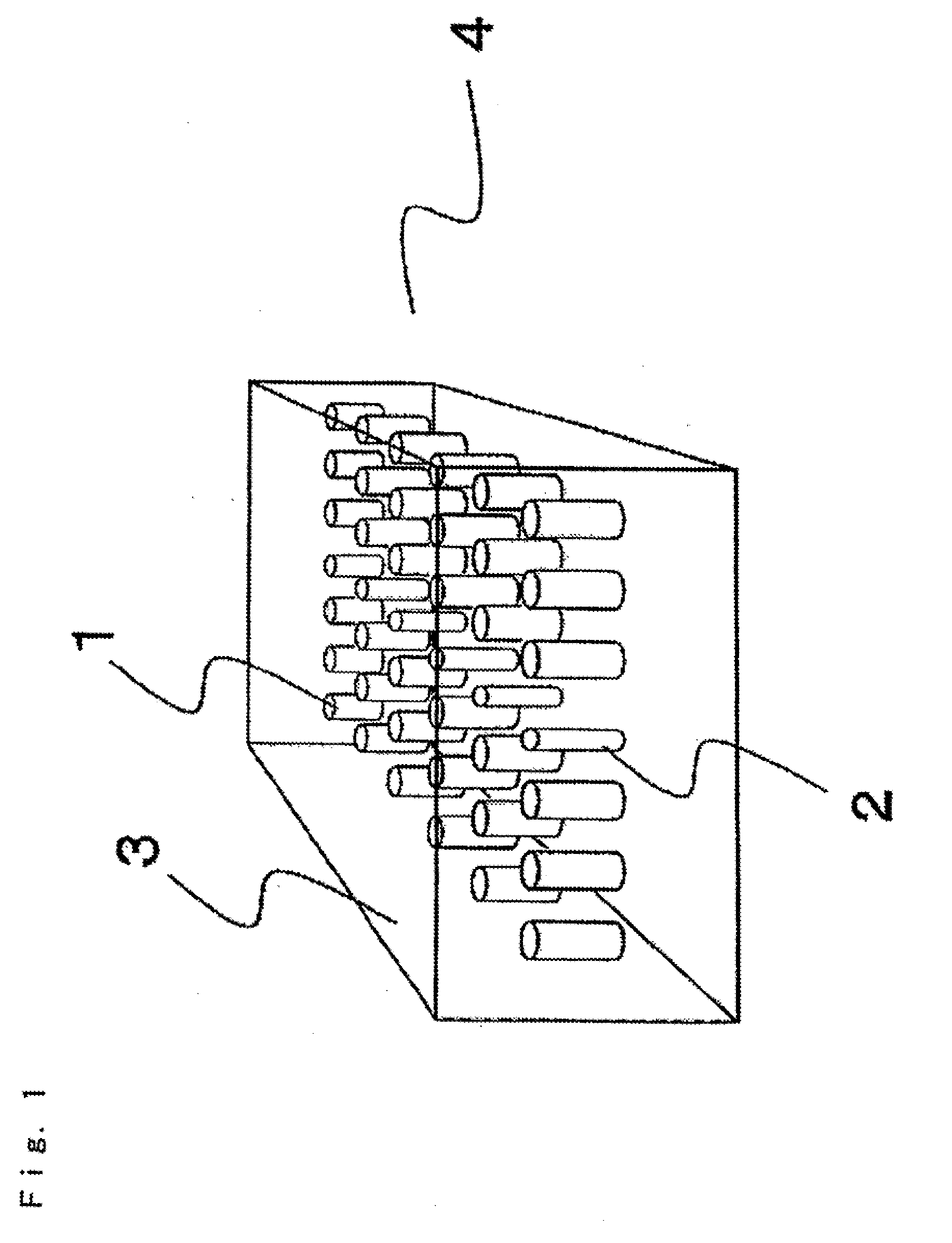
While, generally, light can pass through a photonic crystal, if periodic variation of refractive index within a photonic crystal is sufficiently large, light in a specific frequency band cannot propagate within the photonic crystal.
However, since a three dimensional periodic structure is complex, the manufacturing cost thereof tends to increase.
However, using the above described “resonator stub” results in a problem that, since it resonates only with a specific wavelength in the transmission band of the waveguide thereby operating as a filter, the resonator stub cannot be used when it is desirable to operate it as a filter for lights having a plurality of wavelengths in a wide band.

Method used


Image

  • Photonic crystal element
  • Photonic crystal element
  • Photonic crystal element

Examples


Embodiment Construction

[0030]Next, exemplary embodiments will be described based on the drawings.

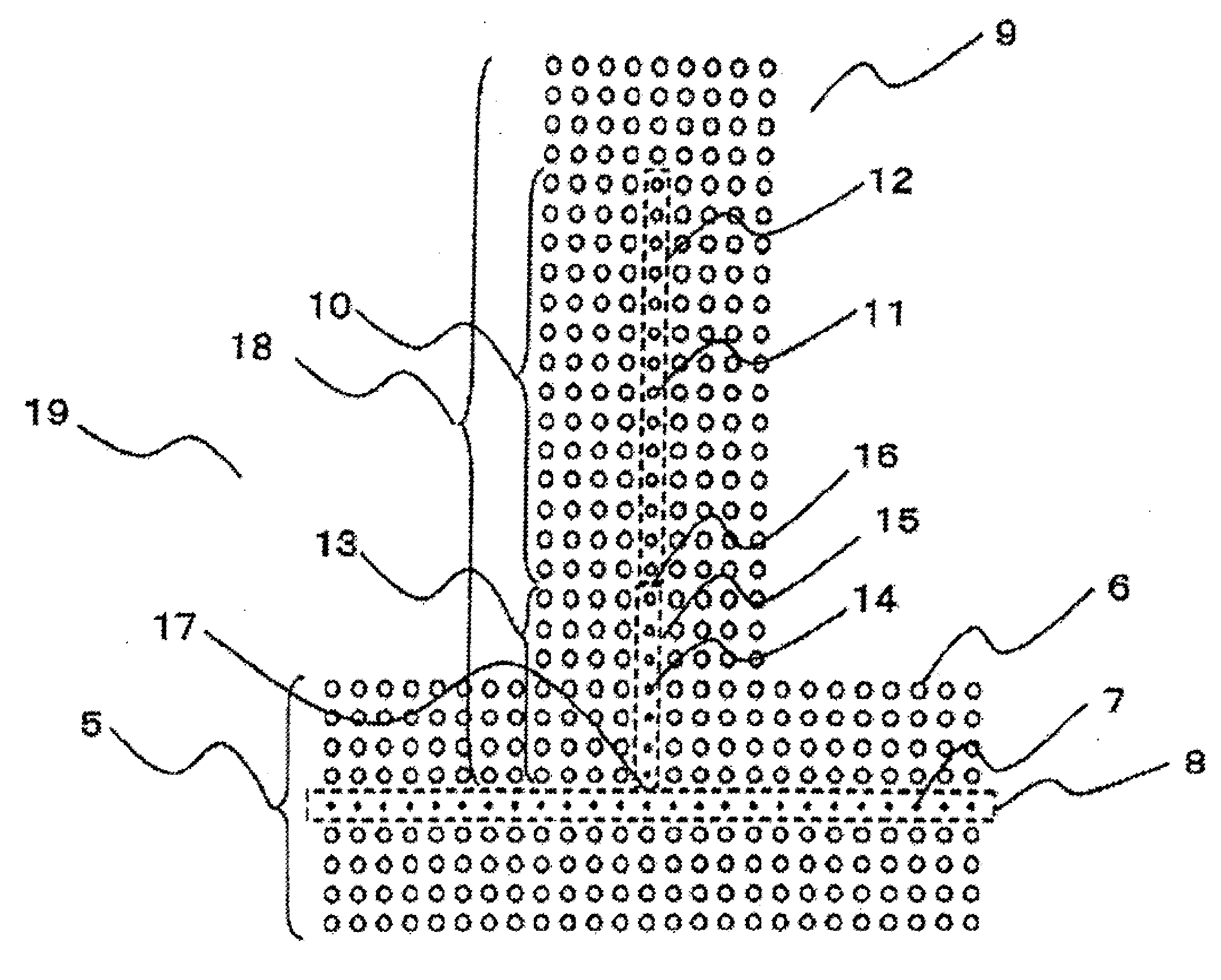
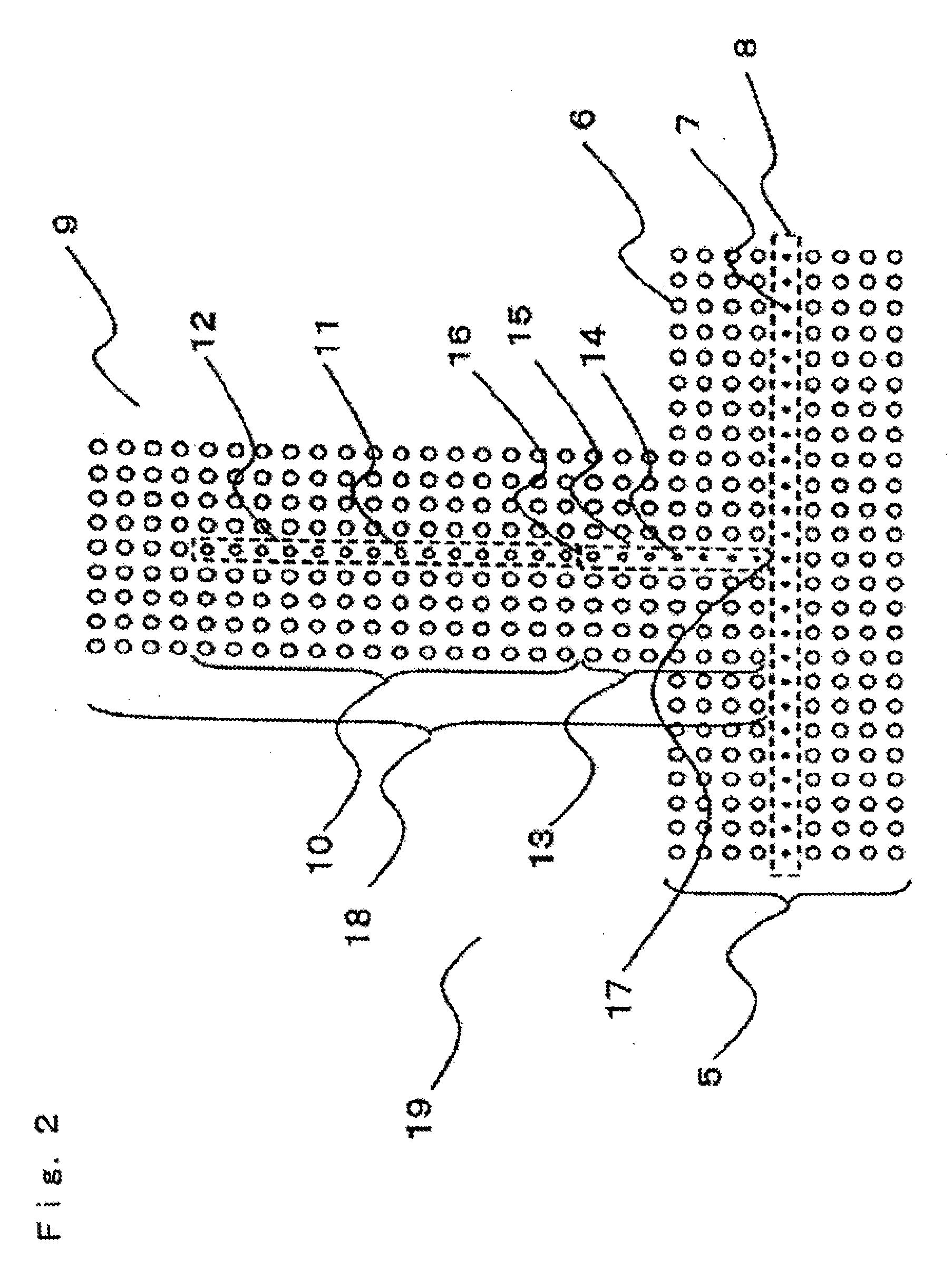
[0031]FIG. 2 is a schematic view to illustrate a first exemplary embodiment.

[0032]As shown in FIG. 2, photonic crystal element 19 of the present exemplary embodiment is in many cases included in an arbitrary pillar-type square-lattice photonic crystal as a part thereof. The periodic lattice of the photonic crystal is a lattice of dielectric pillars having a high refractive index and disposed in a medium of a refractive index smaller than the other part.

[0033]Waveguide 5 in the photonic crystal is included, waveguide 5 being able to guide light having a frequency within a band gap of the photonic crystal. That is, in the photonic crystal, the waveguide which includes a periodic lattice includes first defect 8 which is a dielectric pillar of a small cross-sectional area in the periodic lattice.

[0034]Waveguide 5 has a structure in which a line of pillars of a small cross-sectional area are introduced in a non-def...


PUM


Abstract

A waveguide stub is connected to a pillar-type square-lattice photonic crystal waveguide. Within the waveguide stub, the diameter of a defect is made larger than that of the original photonic crystal waveguide thereby reducing the group velocity of a guided light. The original waveguide and the waveguide stub are smoothly connected via a taper waveguide. Because of low group velocity of light in the waveguide stub, free spectral range (FSR) decreases thereby allowing the size of the waveguide stub to be reduced.

Description

TECHNICAL FIELD[0001]The present invention relates to a photonic crystal element, and particularly to a photonic crystal element having a waveguide structure.BACKGROUND ART[0002]It is desired that a technology appears for realizing an optical integrated circuit in which optical components are integrated like a transistor integrated circuit, in which electronic components are integrated. At present, an optical circuit is assembled by connecting optical components such as optical switches, wavelength filters, 3-dB couplers (optical couplers), etc. via optical waveguides such as optical fibers.[0003]However, if a plurality of optical components can be integrated into a small chip, it is possible to dramatically reduce the volume, power consumption, and manufacturing cost of an optical circuit.[0004]A host of technologies with the aim of realizing an optical integrated circuit have been developed so far, and among them is photonic crystal technology. A photonic crystal element or a phot...

Claims


Application Information

Patent Timeline
Patent Type & Authority Applications(United States)
IPC IPC(8): G02B6/26
CPCB82Y20/00G02B6/1225G02B6/1228G02B6/355G02B6/3596G02F2202/32G02B2006/12119G02B2006/12145G02F1/035G02F1/3137G02B2006/12109
Inventor TOKUSHIMA, MASATOSHI
Owner NEC CORP
Learn More