Methods and apparatus for forming uniform particle layers of phosphor material on a surface

Inactive Publication Date: 2010-11-18
ACHROLUX
View PDF37 Cites 107 Cited by
  • Summary
  • Abstract
  • Description
  • Claims
  • Application Information

AI Technical Summary

Benefits of technology

[0028]Another alternative embodiment of the present invention provides a method for forming a LED encapsulant structure. The method includes forming a LED encapsulant structure body having a surface layer that includes a B-stage polymer, curing the LED encapsulant structure body using a first heating process, forming a layer of an LED phosphor material on the surface layer of the LED encapsulant structure body, softening the surface layer of the LED encapsulant structure body using a second heating process, and causing at least a portion of the LED phosphor material to be at least partially embedded in the surfac

Problems solved by technology

For slurry methods, common or known difficulties in applying phosphor layer to LED chip or package are many, such asVariation of thickness uniformity on surface.
The slurry method usually forms a particle layer with varying thickness, especially applied on non-flat surface.Difficulties in achieving high packing density of thin particles layers.
Therefore, the coated layer contains a high percentage of binder materials, which is typically not a good thermal conductor, increasing the difficulty in dissipating heats for the package.
In electrophoretic deposition (EPD), although a high packing density of phosphor particles can be formed with a thickness less than 20 um, the known difficulties in EP

Method used


Image

  • Methods and apparatus for forming uniform particle layers of phosphor material on a surface
  • Methods and apparatus for forming uniform particle layers of phosphor material on a surface
  • Methods and apparatus for forming uniform particle layers of phosphor material on a surface

Examples


Embodiment Construction

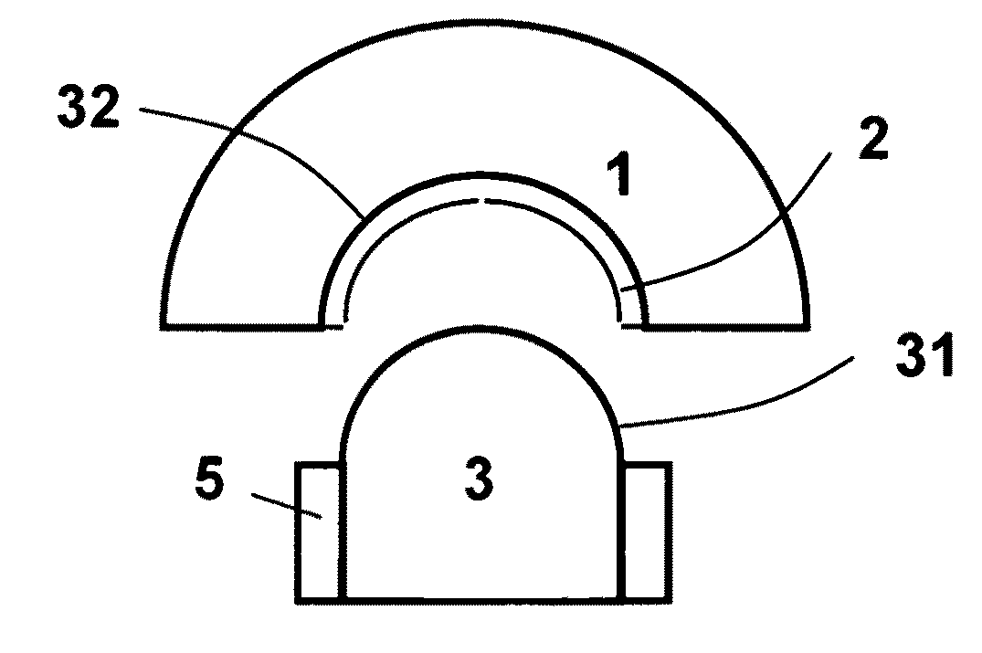
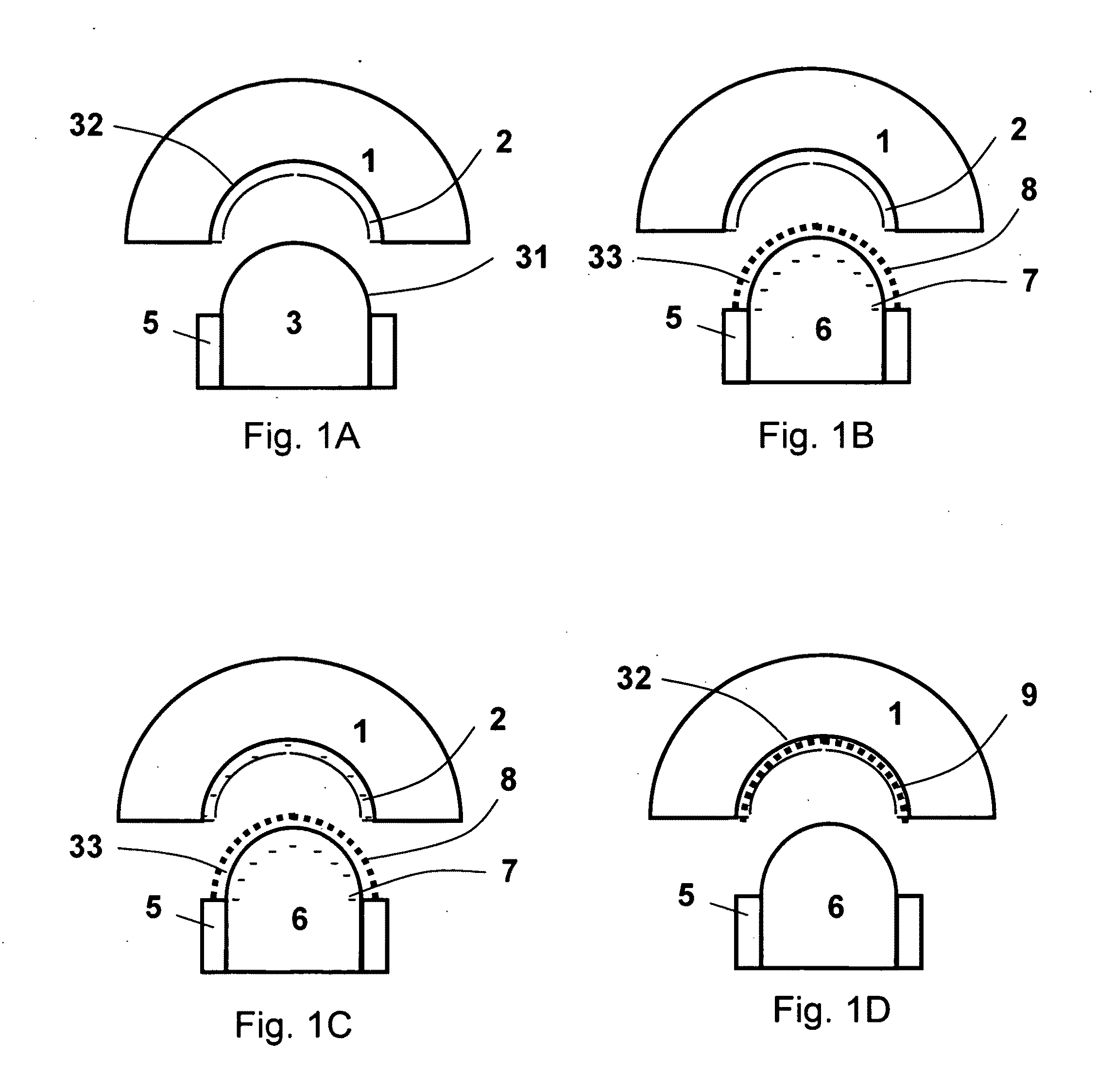
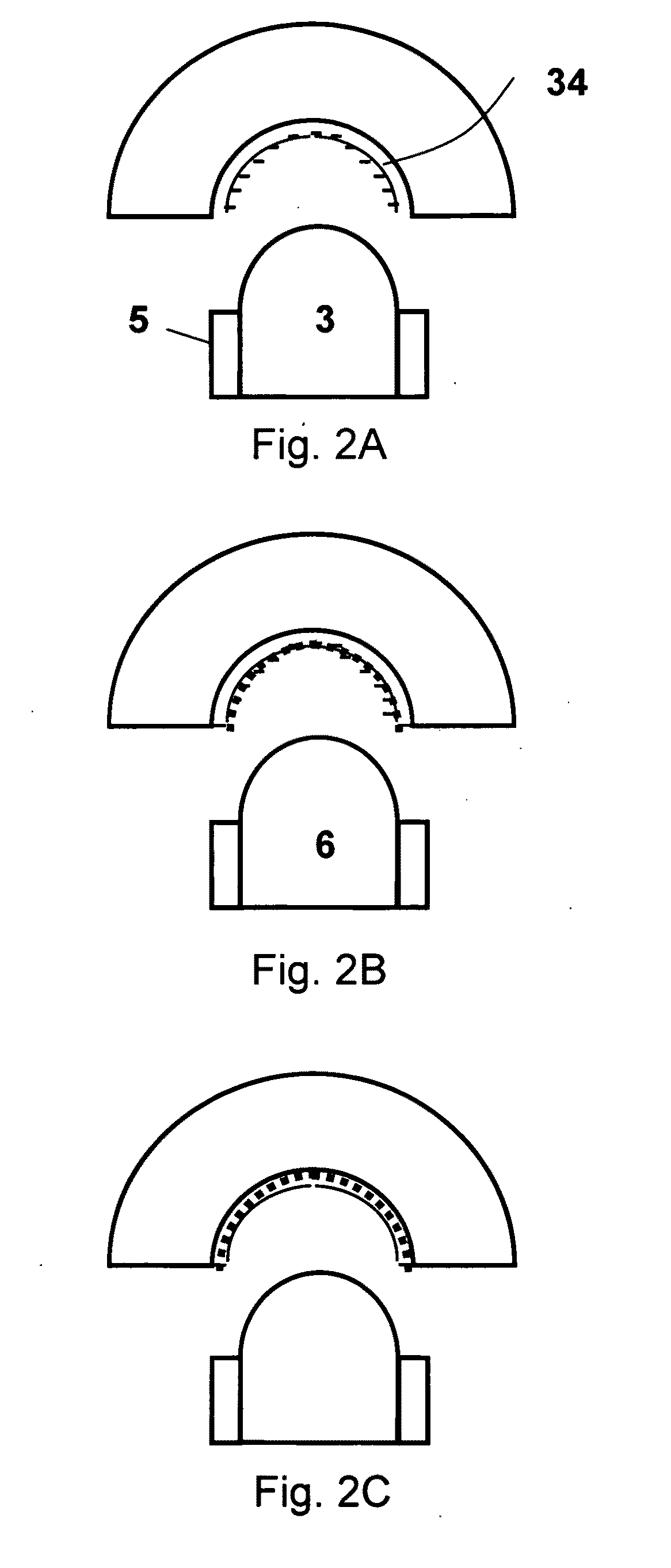
[0051]In the specific examples described herein, phosphors are used for converting or altering light wavelength, e.g., for LED-based light sources. Common phosphors for these purposes include yttrium aluminum garnet (YAG) materials, terbium aluminum garnet (TAG) materials, ZnSeS+ materials, and silicon aluminum oxynitride (SiAlON) materials (such as. α-SiAlON), etc. According to embodiments of the present invention, however, any material that converts or alters wavelength of incident light can be used as a phosphor material. As used herein, the term “phosphor” represents all materials that is capable of converting or altering a wavelength of light to another wavelength, including mixture or combination of different wavelength-converting or wavelength altering materials.

[0052]In some embodiments of the present invention, the coating process does not require keeping powder particles and binder in a liquid suspension form. Phosphor powder particles and binder materials can be coated se...


PUM

PropertyMeasurementUnit
Electric chargeaaaaaaaaaa
Electrical conductoraaaaaaaaaa
Distanceaaaaaaaaaa

Abstract

A method for forming a layer of an LED phosphor material includes disposing a first surface in a proximity of a powder that includes an LED phosphor material, forming electrostatic charges on the first surface, and forming a layer of the LED phosphor material on the first surface at least partially by using the electrostatic charges. In an embodiment, the method includes disposing the first surface in an interior of a chamber and forming an airborne distribution of the powder in the interior of the chamber in a vicinity of the first surface. In another embodiment, the method includes providing a reservoir of the powder and applying to said phosphor powder an electrostatic charge opposite to that of said electrostatic charge on the first surface.

Description

CROSS-REFERENCES TO RELATED APPLICATIONS[0001]This application claims priority to U.S. Provisional Application No. 61 / 216,374, filed May 15, 2009, by Peiching Ling and U.S. Provisional Application No. 61 / 273,129, filed Jul. 30, 2009, by Peiching Ling, both commonly owned and incorporated by reference in their entirety herein for all purposes. This application is also related to concurrently filed U.S. application Ser. No. ______ (Applicant Docket No. LING-090400US) by Peiching Ling and U.S. application Ser. No. ______ (Applicant Docket No. LING-090500US) by Peiching Ling, both of which are commonly owned and incorporated herein by reference in their entirety for all purposes.BACKGROUND OF THE INVENTION[0002]The present invention relates generally to material processing and optical apparatus techniques. More particularly, embodiments of the invention provide methods and systems for forming a layer of material that can be used in an optical device, such as a phosphor layer for a lens ...

Claims


Application Information

Patent Timeline
IPC IPC(8): B05D1/06
CPCC09K11/02C09K11/7774C23C24/06H05B33/10H01L33/507H01L33/508H01L2933/0041C23C24/08H01L33/50H01L33/52
Inventor LING, PEICHING
Owner ACHROLUX
Why Eureka
Try Eureka