Multiple junction photovolatic devices and process for making the same

a photovolatic device and multi-junction technology, applied in the field of photovoltaic devices, can solve the problems of difficult photovoltaic devices, low conversion efficiency of conventional a-si:h based cells, and inability to properly absorb the radiant energy of the ultra violet and blue part of the solar spectrum, and achieve the effect of high-rate chemical vapor deposition process

Inactive Publication Date: 2010-12-02
CHEN YUNG T
View PDF3 Cites 34 Cited by
  • Summary
  • Abstract
  • Description
  • Claims
  • Application Information

AI Technical Summary

Benefits of technology

[0007]The present invention addresses the drawbacks of conventional single junction photovoltaic devices noted above and provides improved devices having multiple photoelectric cells arranged in a tandem configuration and a high rate chemical vapor deposition process for making the same.

Problems solved by technology

Conversely, if the band gap energy is low, then a significant amount of the radiant energy from the ultra violet and blue part of the solar spectrum cannot be properly absorbed by the cell and is lost in the form of heat.
It is difficult for photovoltaic devices having only one photoelectric conversion cell (i.e. single junction) to fully utilize the entire solar spectrum in an efficient manner.
However, conventional a-Si:H based cells are plagued by comparatively low conversion efficiencies of less than 7% and light-induced degradation also known as Staebler-Wronski effect.
Because nc-Si:H has lower optical absorption coefficient in the visible range of the solar spectrum, however, the nc-Si:H layer in solar cells needs to be 3 to 10 times thicker than that required of a-Si:H, making nc-Si:H based cells comparatively more costly to produce using conventional film deposition techniques such as chemical vapor deposition (CVD).
Although a-Si:H based photovoltaic devices have been commercially produced by PECVD for years, the production of comparatively thicker nc-Si:H layers by conventional PECVD is disadvantageously limited by the PECVD deposition rate.
As the film forming rate of nc-Si:H is increased by increasing the RF power input, however, the bombardment of the growing nc-Si:H film on the substrate by highly energized ions also increases, thereby generating film structural defects which have deleterious effects on electrical properties of the film.
A problem associated with conventional single junction photovoltaic devices which have only one photoelectric conversion cell as described above is that these devices cannot fully utilize the entire solar spectrum in an efficient manner.
Another problem associated with forming of nano-crystalline silicon semiconductor layers for photovoltaic devices as described above is that the conventional PECVD method is comparatively slow and is thus not cost effective for production of nano-crystalline silicon based photovoltaic devices, particularly devices comprising multiple cells.

Method used


Image

  • Multiple junction photovolatic devices and process for making the same
  • Multiple junction photovolatic devices and process for making the same
  • Multiple junction photovolatic devices and process for making the same

Examples


Embodiment Construction

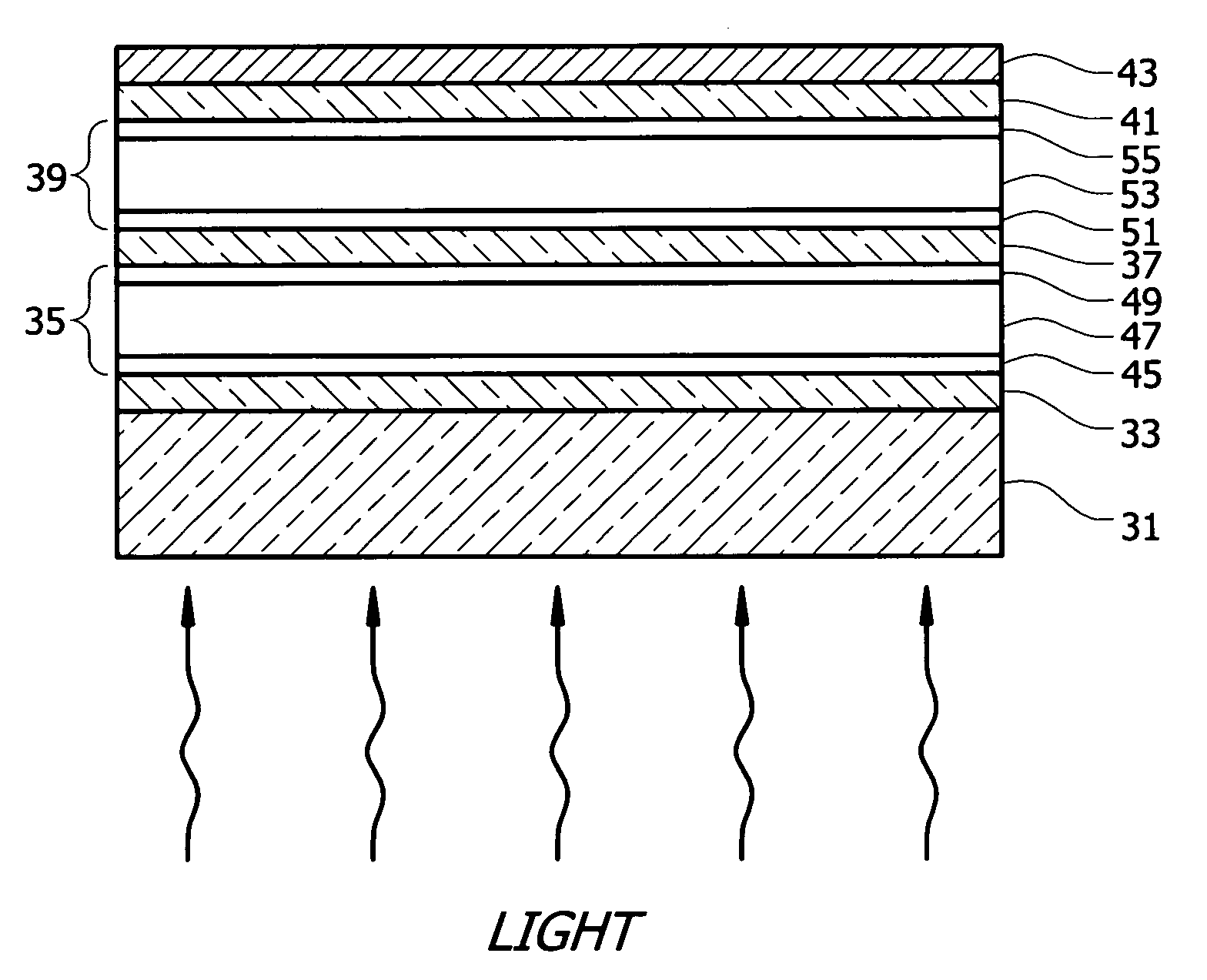
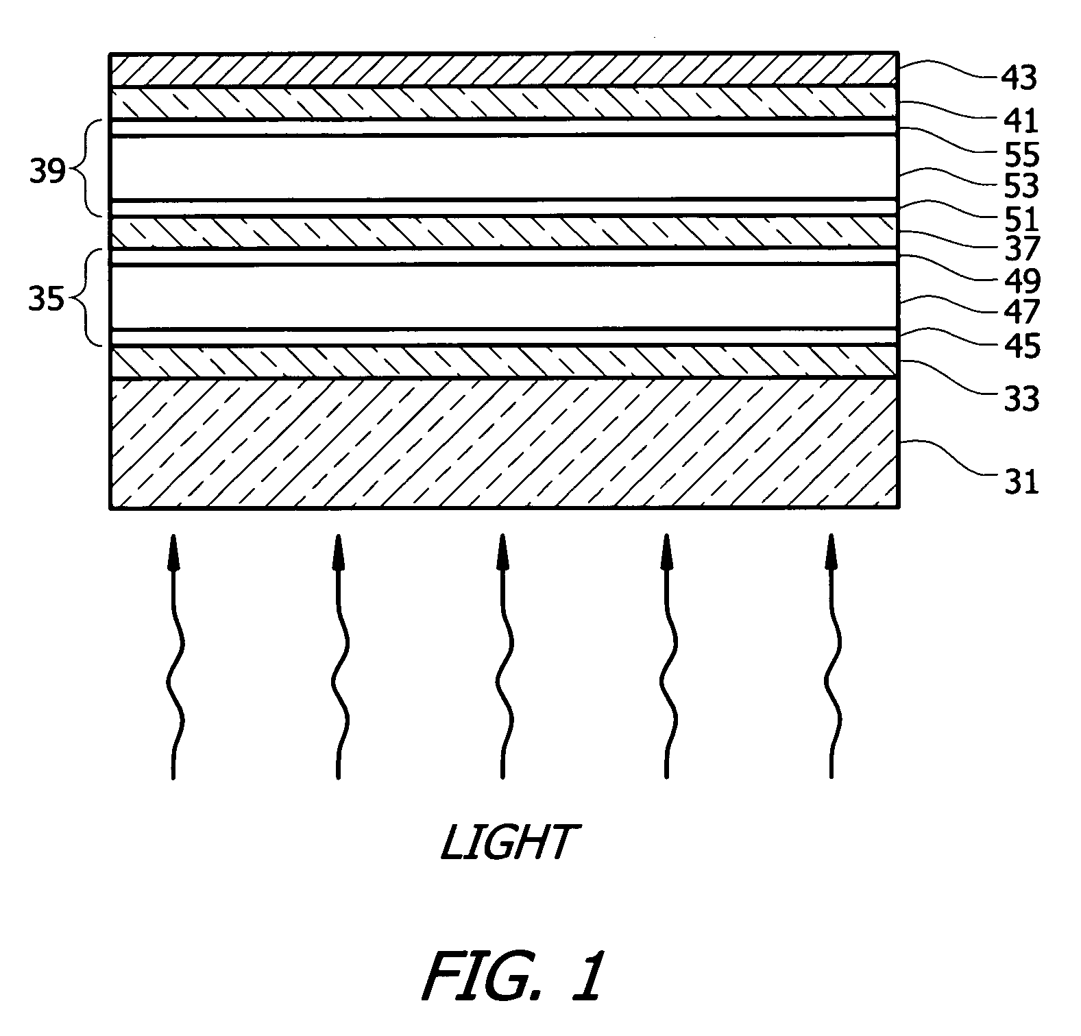
[0022]The present invention overcomes the inability of the conventional single junction photovoltaic device to effectively utilize the entire solar spectrum by the spectrum splitting or multiple band gap approach, in which multiple cells having different band gap energies are arranged in a tandem configuration to effectively absorb photons from a wider range of the solar spectrum.

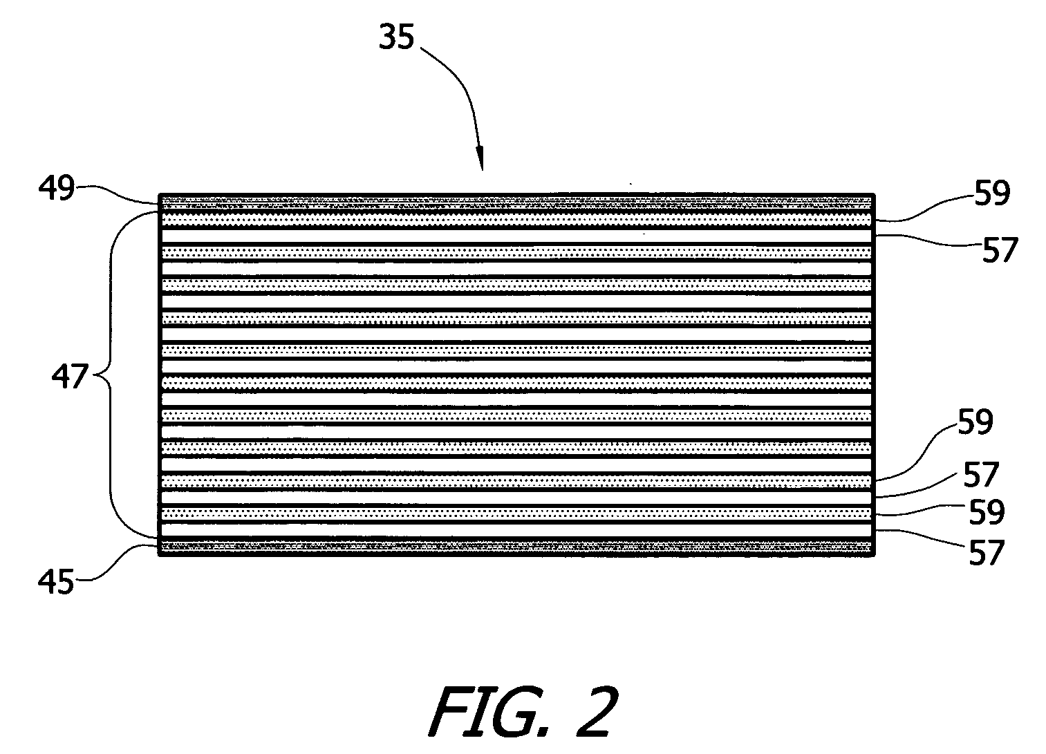
[0023]The present invention as applied to a double junction photovoltaic device having two photoelectric conversion cells arranged in a tandem configuration will now be described with reference to FIG. 1. Referring now to FIG. 1, the illustrated device has an optically transparent dielectric substrate 31, through which radiant energy or sunlight enters the device; a layer of a textured transparent front contact 33 formed of a transparent conductive oxide (TCO) material disposed on the substrate 31; a first photoelectric conversion cell 35 having a band gap energy in the range of about 1.6 eV to about 1.9 eV...


PUM


Abstract

A photovoltaic device having multiple photoelectric conversion cells disposed in a tandem configuration and a chemical vapor deposition method for fabricating the same are disclosed. Each photoelectric conversion cell has a different band gap energy and includes a p-type semiconductor layer, an intrinsic semiconductor layer and an n-type semiconductor layer in sequential touching contact. Each semiconductor layer is formed of a nano-crystalline semiconductor containing silicon as a principal constituent. The semiconductor layer may be deposited by a novel chemical vapor deposition method which utilizes plasma and laser energies simultaneously to decompose a film forming gas, thereby forming a semiconductor film on a substrate. The chemical vapor deposition process may be carried out on a continuously conveying substrate, thereby permitting high throughput production of the photovoltaic device.

Description

FIELD OF THE INVENTION[0001]The present invention relates to photovoltaic devices having at least two photoelectric conversion cells arranged in a tandem configuration and more particularly to cells made of silicon and silicon alloys and process for making the same.BACKGROUND OF THE INVENTION[0002]Photovoltaic technology offers great potential as an alternative source of electrical energy. Conventional thin film photovoltaic devices for converting optical energy into electrical energy usually include a photoelectric conversion cell interposed between two electrodes. The photoelectric conversion cell usually comprises at least two layers of semiconductors films having opposite conductivity types, i.e. p-type and n-type. The cell may also have three semiconductor layers having different conductivity types to thereby form a p-i-n junction. The photoelectric conversion efficiency of a cell markedly depends on the band gap energy of the main semiconductor layer. If the band gap energy is...

Claims


Application Information

Patent Timeline
Patent Type & Authority Applications(United States)
IPC IPC(8): H01L31/042H01L21/20
CPCH01L21/02529H01L21/02532H01L21/02573Y02E10/548H01L31/035218H01L31/076H01L31/1812H01L21/0262
Inventor CHEN, YUNG T.
Owner CHEN YUNG T
Why Eureka
Try Eureka