

Dielectric layer for an electronic device
a technology of dielectric layer and electronic device, which is applied in the direction of thermoelectric device, semiconductor/solid-state device details, plastic/resin/waxes insulator, etc., can solve the problems of high operating voltage, low mobility, and difficult purification
- Summary
- Abstract
- Description
- Claims
- Application Information
AI Technical Summary
Benefits of technology
Problems solved by technology
Method used
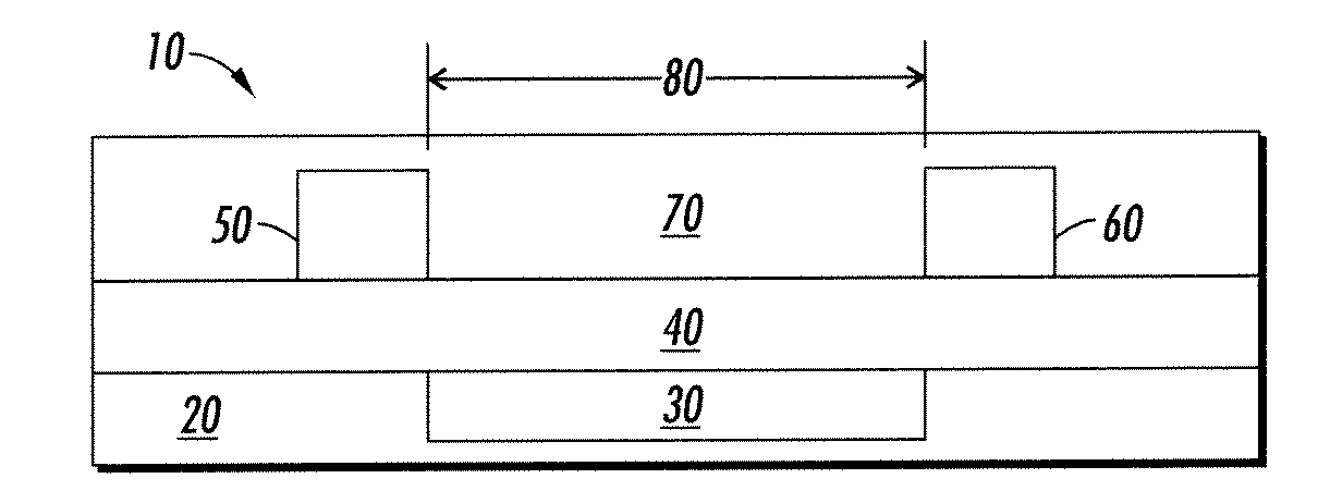
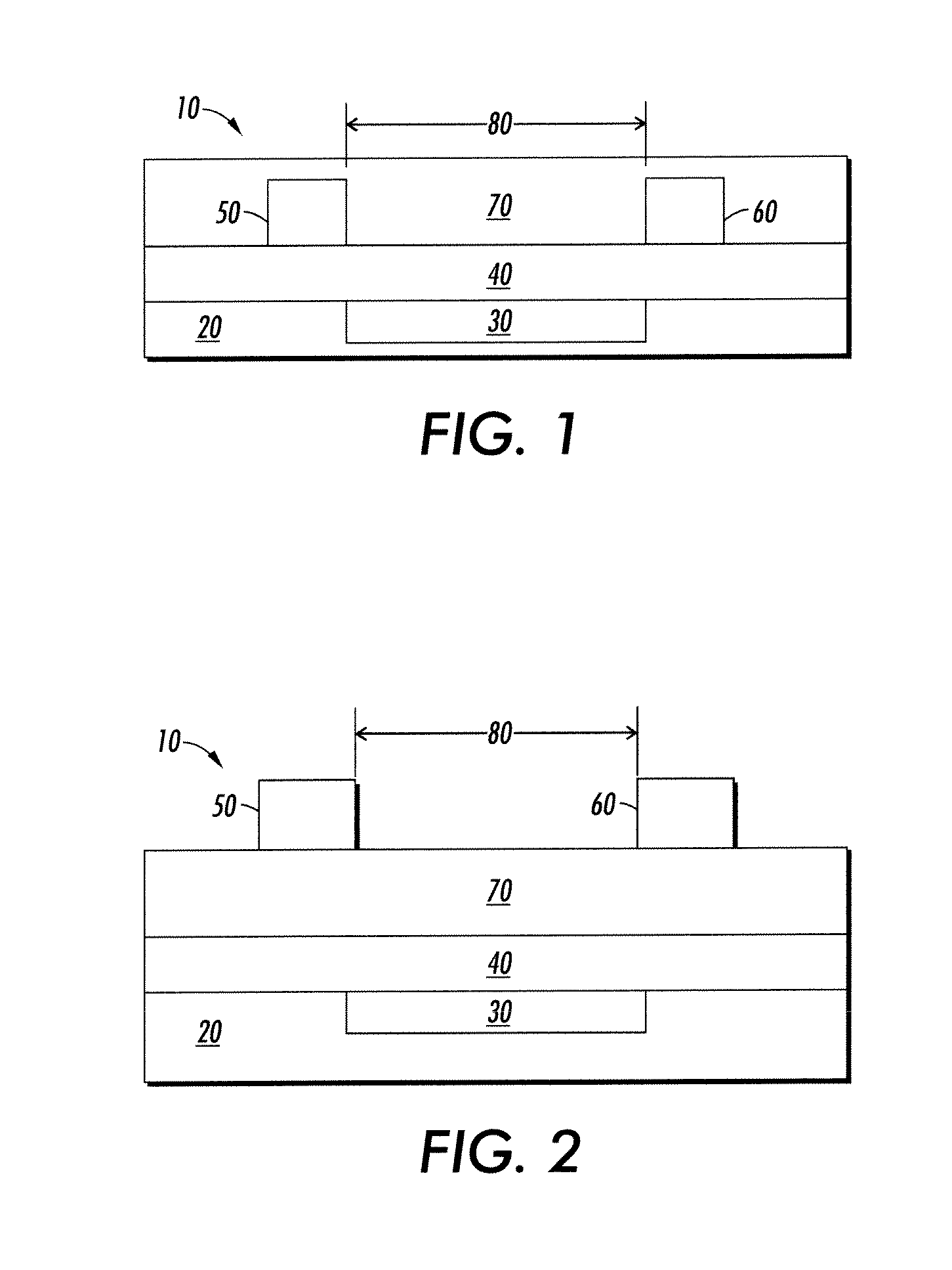
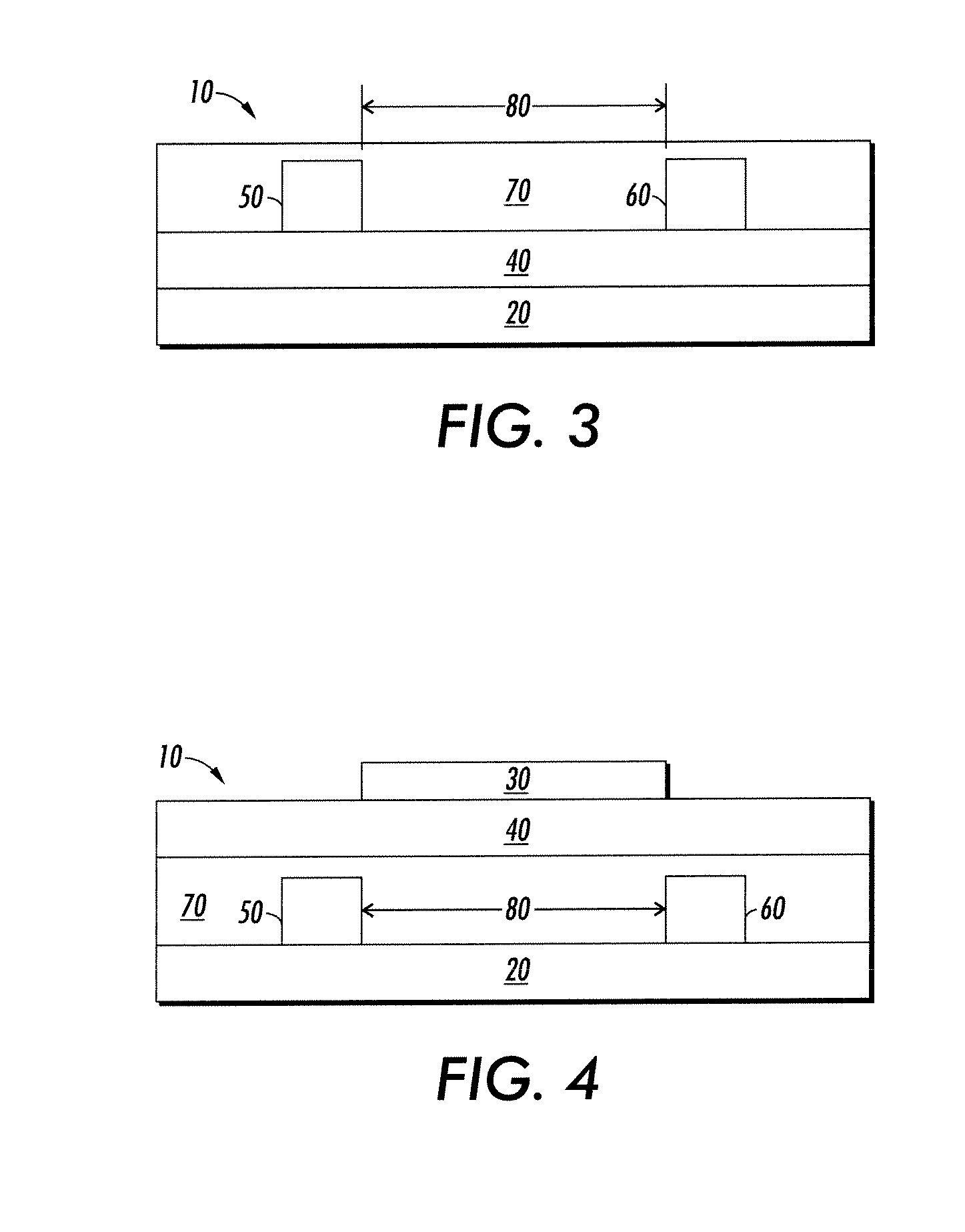
Image

Examples
example 1
[0070]5,5′,6,6′-Tetrahydroxy-3,3,3′,3′ tetramethyl-1,1′spirobisindane was purchased from Alfa Aesar. The spiro compound was dissolved in propylene glycol methyl ether acetate at a 12 wt % loading, together with 6 wt % melamine-formaldehyde resin as crosslinking agent, and a small amount of toluene sulfonic acid as the acid catalyst. The solution was filtered with a 0.2 micron syringe filter and spin-coated at 1000 rpm on a glass slide. The film (˜200 nm thick) was baked at 120° C. for 30 minutes. The resulting film was very uniform and robust, and was resistant to most solvents, including dichlorobenzene.
example 2
[0071]4,4′-(1,4-phenylenediisopropylidene)bisphenol was used in this example. This molecular glass was dissolved in propylene glycol methyl ether acetate at a 12 wt % loading, together with 6 wt % melamine-formaldehyde resin as crosslinking agent, and a small amount of toluene sulfonic acid as the acid catalyst. The solution was filtered with a 0.2 micron syringe filter and spin-coated at 1000 rpm on a glass slide. The film (˜200 nm thick) was baked at 120° C. for 30 minutes. The resulting film was very uniform and robust, and was resistant to most solvents, including dichlorobenzene.
PUM
| Property | Measurement | Unit |
|---|---|---|
| Dielectric polarization enthalpy | aaaaa | aaaaa |
| Molecular weight | aaaaa | aaaaa |
| Glass transition temperature | aaaaa | aaaaa |
Abstract
Description
Claims
Application Information