

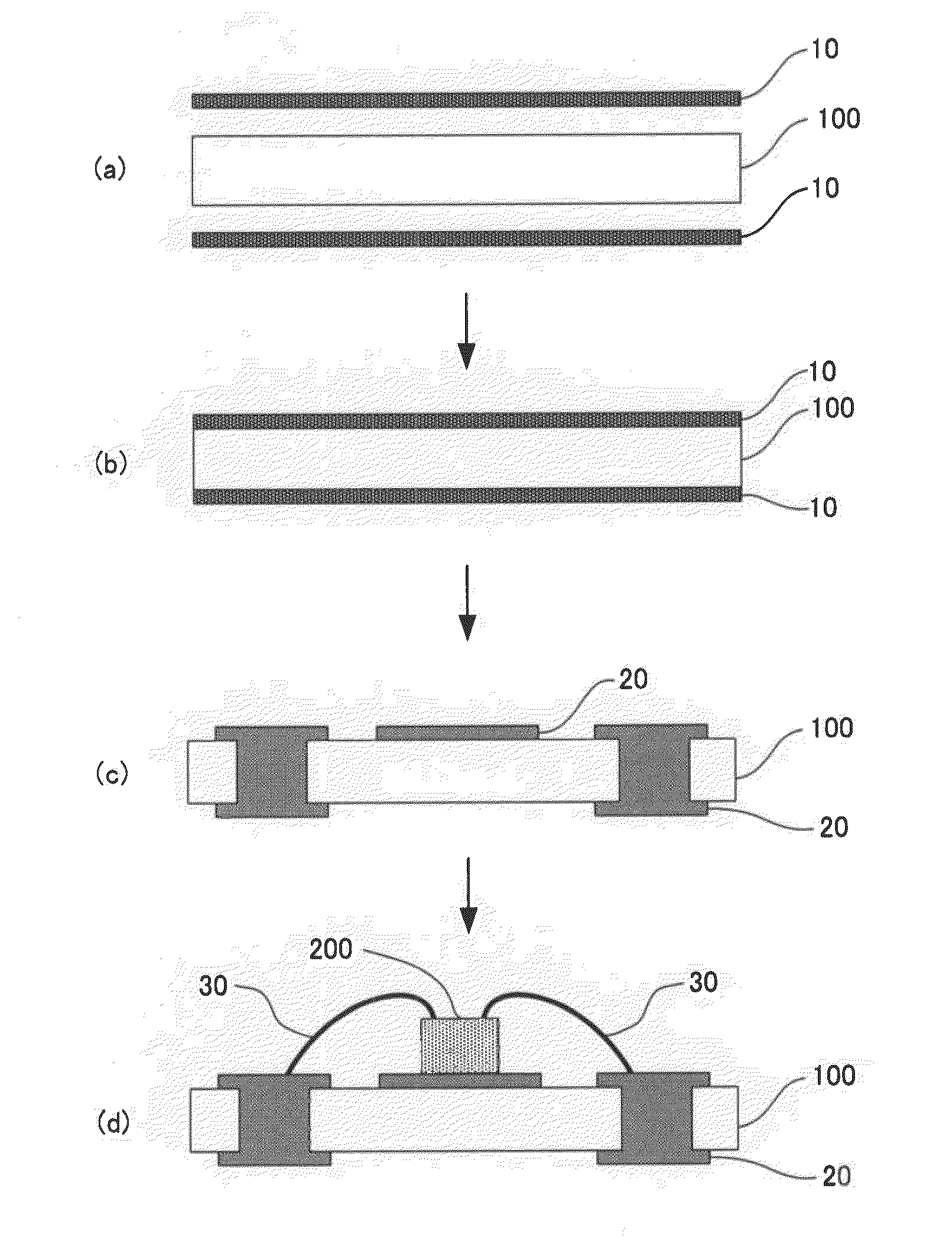
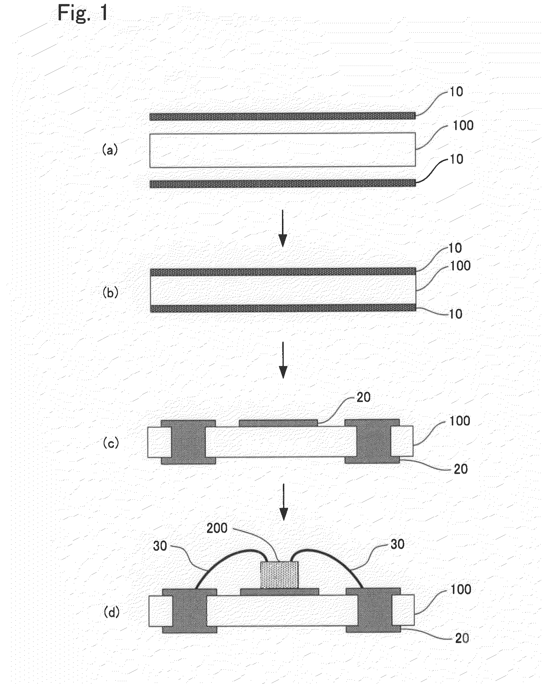
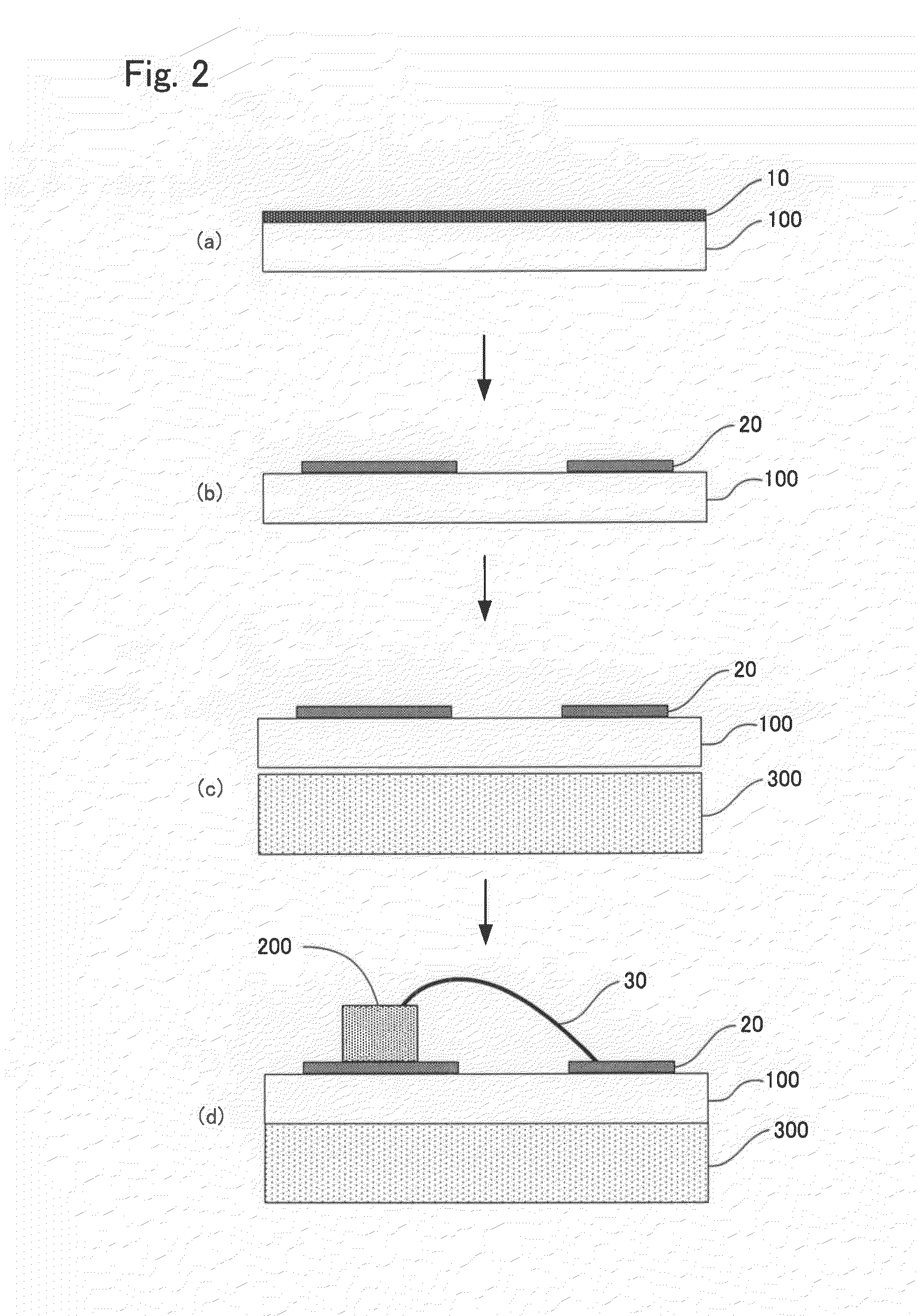
Metal laminated body, led-mounted substrate, and white film
a technology of led-mounted substrates and laminated bodies, which is applied in the direction of cathode ray/electron stream lamps, inorganic insulators, incandescent lamp details, etc., can solve the problems of difficult future general lighting and substrate use, and limit the use of ceramic substrates for larger-size and lower-profile products, etc., to achieve excellent dimensional stability, high reflectance, and high thermal resistance
- Summary
- Abstract
- Description
- Claims
- Application Information
AI Technical Summary
Benefits of technology
Problems solved by technology
Method used
Image

Examples
example 1
[0097]A thermoplastic resin composition obtained by mixing: 100 parts by mass of a resin composition comprising 60 mass % of polyether ether ketone resin (“PEEK 450G”, Tm=335° C.) and 40 mass % of amorphous polyetherimide resin (“ULTEM 1000”); 30 parts by mass of a titanium oxide (average particle diameter: 0.23 μm, treated with alumina and a silane coupling agent) produced by chlorine method; and 21 parts by mass of synthetic mica having an average particle diameter of 5 μm and an average aspect ratio of 50 was melt-kneaded. Then, the melt-kneaded thermoplastic resin composition was formed into a 100 μm thick film using an extruder having T-dies at a set temperature of 380° C. The evaluation results are shown in Table 1.
example 2
[0098]Except for using a resin mixture comprising: 40 mass % of polyether ether ketone resin (“PEEK 450G”, Tm=335° C.); and 60 mass % of amorphous polyetherimide resin (“ULTEM 1000”), Example 2 was carried out in the same manner as Example 1 to produce a 100 μm thick film. The evaluation results are shown in Table 1.
example 3
[0099]Except for using a thermoplastic resin composition obtained by mixing: 35 parts by mass of titanium oxide; and 30 parts by mass of a synthetic mica having an average particle diameter of 5 μm and an average aspect ratio of 50, Example 3 was carried out in the same manner as Example 1 to produce a 100 μm thick film. The evaluation results are shown in Table 1.
PUM
| Property | Measurement | Unit |
|---|---|---|
| reflectance | aaaaa | aaaaa |
| reflectance | aaaaa | aaaaa |
| average particle diameter | aaaaa | aaaaa |
Abstract
Description
Claims
Application Information