Method for manufacturing semiconductor laser diode

a laser diode and semiconductor technology, applied in the direction of lasers, semiconductor devices, semiconductor lasers, etc., can solve the problem of dull side surface of the opening in the resin layer, and achieve the effect of effectively preventing breakag

Active Publication Date: 2010-12-02
SUMITOMO ELECTRIC IND LTD
View PDF0 Cites 16 Cited by
  • Summary
  • Abstract
  • Description
  • Claims
  • Application Information

AI Technical Summary

Benefits of technology

[0014]Because of the dulled side surface of the opening in the resin layer, the wiring formed so as to come in contact with the semiconductor stack and to

Problems solved by technology

Then, the tri-step etching of the embodiment may make t

Method used


Image

  • Method for manufacturing semiconductor laser diode
  • Method for manufacturing semiconductor laser diode
  • Method for manufacturing semiconductor laser diode

Examples


first embodiment

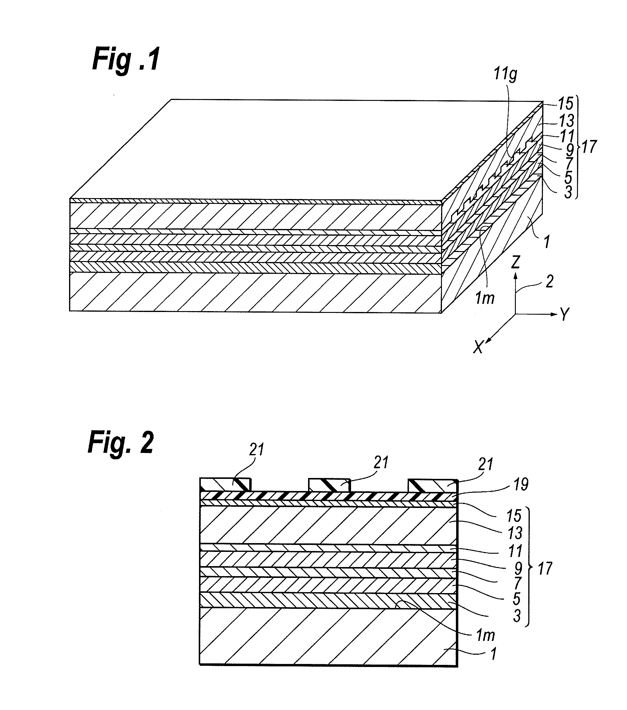
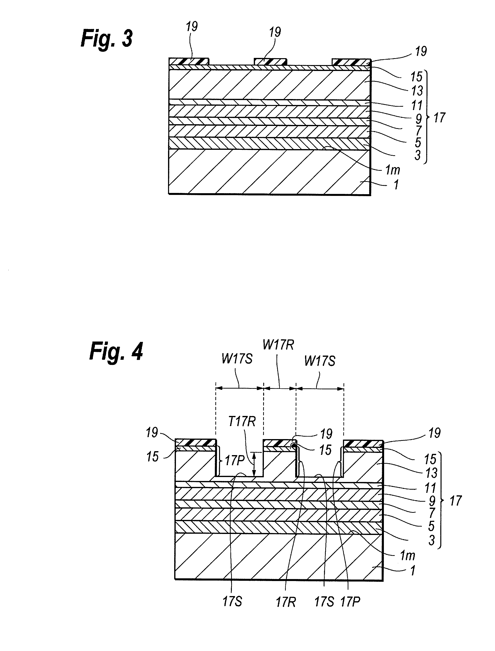
[0032]First, a process to form an LD 100 and a structure according to the first embodiment of the invention will be described by concentrating on an LD with the ridge waveguide structure. FIG. 1 is a schematic cross drawing of the LD according to the present embodiment; FIGS. 2 to 11 sequentially explain the process of the LD by the cross sections thereof; and FIG. 12 is a perspective view of the LD 100.

[0033](Layer Growth)

[0034]The process according to the embodiment first grows a plurality of semiconductor layers by, for instance, a conventional metal organic chemical vapor deposition (MOCVD) technique on a primary surface 1m of the semiconductor substrate 1. The stacked semiconductor layers include a lower cladding layer 3, a lower optical confinement layer 5, an active layer 7, an upper optical confinement layer 9, a grating layer 11, an upper cladding layer 13 and a contact layer 15 in this order on the semiconductor substrate 1. The explanation presented below assumes that dir...

second embodiment

[0060]Next, another process and structure of an LD with the buried hetero-structure will be described as the second embodiment of the present invention.

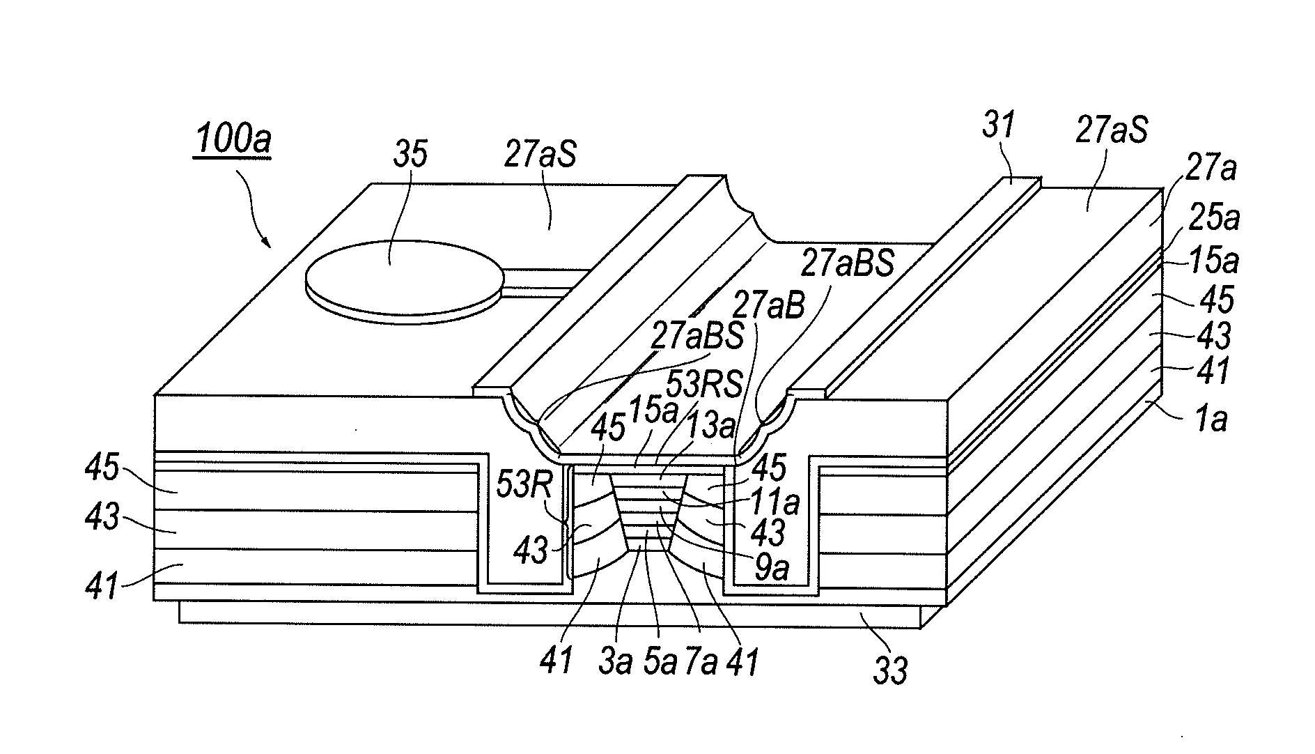
[0061]The process is different from those of the first embodiment in points of the layer growth and the formation of the striped structure. FIG. 13 schematically illustrates a process to stack semiconductor layers for the other LD according to the second embodiment of the invention; FIG. 14 shows a process to from the striped structure; and FIG. 15 is a perspective view of the completed LD 100a of the second embodiment.

[0062](Layer Growth)

[0063]As illustrated in FIG. 13, the stacking of the semiconductor layers includes, on the primary surface 1am of the semiconductor substrate 1a, a lower cladding layer 3a, a lower optical confinement layer 5a, an active layer 7a, an upper optical confinement layer 9a, a grating layer 11a and an upper cladding layer 13a in this order. These layers, 3a to 13a, may be grown by the MOCVD technique as t...


PUM


Abstract

A method for manufacturing an LD is disclosed. The LD has a striped structure including an optical active region. The striped structure is buried with resin, typically benzo-cyclo-butene (BCB). The method to form an opening in the BCB layer has tri-steps etching of the RIE. First step etches the BCB layer partially by a mixed gas of CF4 and O2, where CF4 has a first partial pressure, second step etches the photo-resist patterned on the top of the BCB layer by a mixed gas of CF4 and O2, where CF4 in this step has the second partial pressure less than the first partial pressure, and third step etches the BCB left in the first step by mixed gas of CF4 and O2, where CF4 in this step has the third partial pressure greater than the second partial pressure.

Description

BACKGROUND OF THE INVENTION[0001]1. Field of the Invention[0002]The present invention relates to a method for manufacturing a semiconductor laser diode (hereafter denoted as LD), in particular, the invention relates to a method to form a dulled side surface of an opening to provide an electrode of the LD.[0003]2. Related Background Art[0004]A Japanese Patent Application published as JP-2003-298190A has disclosed an LD with the ridge waveguide structure. Such an LD with the striped structure like the ridge waveguide often causes damage to the striped structure during the process. Accordingly, the LD disclosed therein has provided a pair of protrusion with a height greater than a height of the ridge in both sides of the ridge. The protrusion provided in both side of and apart from the ridge may operate as a protection means for the striped structure.[0005]However, the protrusion structure is necessary to carry out several process steps, namely, first forming a patterned photo-resist b...

Claims


Application Information

Patent Timeline
IPC IPC(8): H01S5/22H01L33/00H01S5/12
CPCH01S5/0425H01S5/12H01S5/2086H01S5/22H01S5/2213H01S5/2214H01S5/2222H01S5/2231H01S5/2275H01S2301/176H01S5/04254
Inventor YAGI, HIDEKIKOYAMA, KENJIYOSHINAGA, HIROYUKIISHIHARA, KUNIAKI
Owner SUMITOMO ELECTRIC IND LTD
Why Eureka
Try Eureka