Semiconductor light emitting element and method for manufacturing the same

Inactive Publication Date: 2010-12-09
MITSUBISHI CHEM CORP
View PDF4 Cites 36 Cited by
  • Summary
  • Abstract
  • Description
  • Claims
  • Application Information

AI Technical Summary

Benefits of technology

[0056]According to the present invention, there can be provided a semiconductor light-emitting element in which crystallinity in a thin-film crystal layer is improved and a crystalline state is less deteriorated and which can meet the requirement for a higher output and a higher luminous efficiency, by forming an insulating film having a crystal quality improving layer as described above. Additionally, by forming an insulating film with an extremely low reflectance as a multilayer film containing an antireflection layer, a light emitted from the thin-film crystal layer of the semiconductor light-emitting element can be extracted through the insulating film. Thus, compared with a conventional semiconductor light-emitting element having an insulating film mainly exerting reflection function, a spatial radiant flux density above the light-emitting element is reduced, even when the total radiation flux is equal. That is, it can be expected that a flip-chip type semiconductor light-emitting element having an insulating film with an extremely low reflectance allows for light emission from, not only the top of the element, all directions of the element such as a sidewall and an electrode side.
[0057]Therefore, the light-emitting element of the present

Problems solved by technology

However, a conventional light-emitting element, particularly a light-emitting element based on a flip-chip type mount, has a configuration in which most of the light generated within the element is extracted from the substrate side for the opposite side to the reflection electrode in, for example, an element without a substrate), so that the light distribution properties of the extracted light is significantly biased, resulting in increase in a spatial radiant flux density above the light-emitting element.
Excessive increase in a spatial energy density due to bias of the light distribution properties for the l

Method used


Image

  • Semiconductor light emitting element and method for manufacturing the same
  • Semiconductor light emitting element and method for manufacturing the same
  • Semiconductor light emitting element and method for manufacturing the same

Examples


Example

Example 1

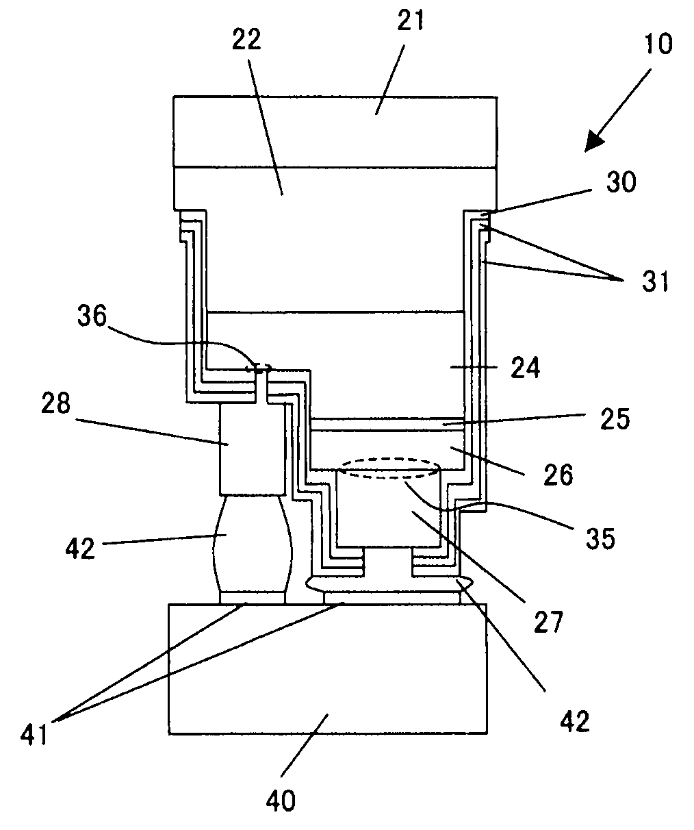
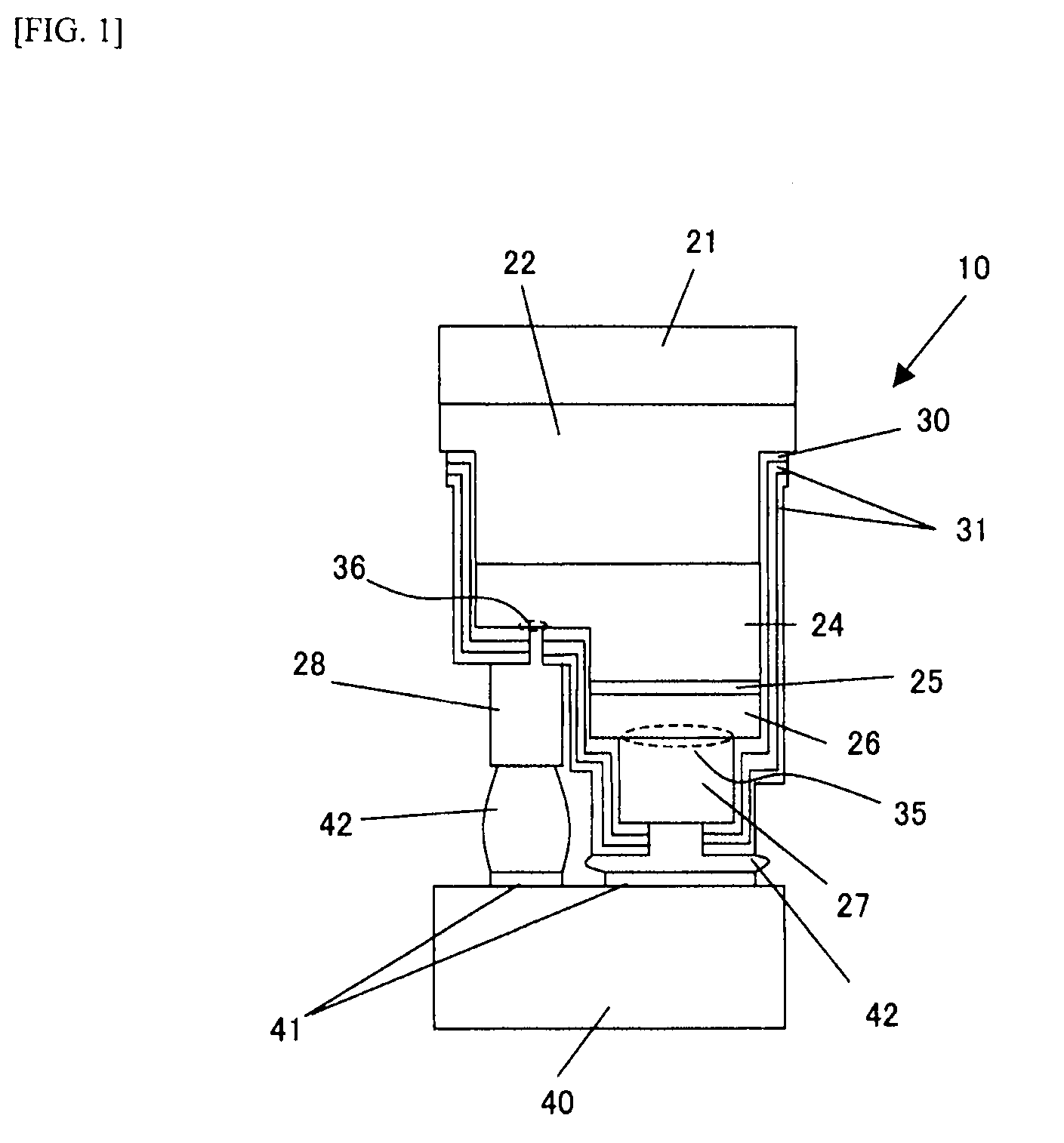
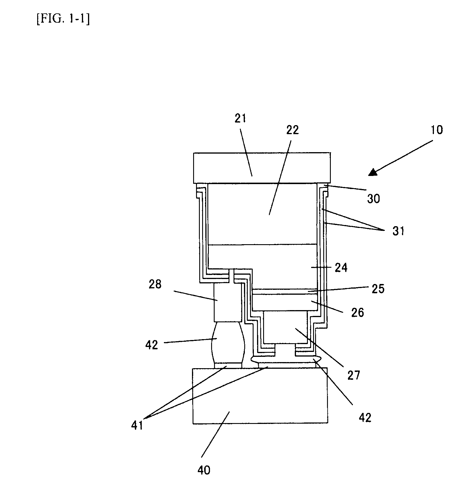
[0261]A light-emitting element shown in FIG. 10 was prepared by the procedure described below. See FIGS. 3 to 8 as relevant process drawings.

[0262]There was prepared a c+plane sapphire substrate 21 with a thickness of 430 μm, on which were formed undoped GaN grown at a low temperature to a thickness of 10 nm as a first buffer layer 22a using MOCVD and then undoped GaN as a second buffer layer 22b to a thickness of 4.0 μm at 1040° C.

[0263]Furthermore, an Si doped (Si concentration: 5×1018 cm−3) GaN layer was formed to a thickness of 4.5 μm as the first-conductivity-type (n-type) cladding layer 24. Furthermore, as the active layer structure 25, were alternately deposited undoped GaN layers to 13 nm as a barrier layer at 860° C. and undoped In0.06Ga0.94N layers as a quantum well layer to 2 nm at 720° C., such that 8 quantum well layers in total were formed and both sides were barrier layers. Then, was formed Mg doped (Mg concentration: 5×1019 cm−3) Al0.2Ga0.8N as the second-co...

Example

Example 2

[0287]A light-emitting element was manufactured as described in Example 1, except that an insulating film was formed such that a crystal quality improving layer made of SiNx had a film thickness of 30 nm and an antireflection layer made of SiOx had a film thickness of 50 nm for adjusting a reflectance of a light vertically entering the insulating film from the thin-film crystal layer side to 0.02% and SiNx was not formed as the uppermost layer of the insulating film.

[0288]FIG. 12 is a graph showing relationship between an insulating-film reflectance at a wavelength of 405 nm and a film thickness of an antireflection layer (SiOx) when on GaN is deposited a crystal quality improving layer made of SiNx to a film thickness of 30 nm, on which is further deposited an antireflection layer made of SiOx to form an insulating film. The refractive indices at a wavelength of 405 nm for SiNx and SiOx used in this calculation were 1.92 and 1.45, respectively, from the preliminary experim...

Example

Example 3

[0291]A light-emitting element was manufactured as described in Example 1, except that an insulating film was formed such that a crystal quality improving layer made of SiNx had a film thickness of 10 nm and an antireflection layer made of SiOx had a film thickness of 62 nm for adjusting a reflectance of a light vertically entering the insulating film from the thin-film crystal layer side to 0.6% and SiNx was not formed as the uppermost layer of the insulating film.

[0292]FIG. 13 is a graph showing relationship between an insulating-film reflectance at a wavelength of 405 nm and a film thickness of an antireflection layer (SiOx) when on GaN is deposited a crystal quality improving layer made of SiNx to a film thickness of 10 nm, on which is further deposited an antireflection layer made of SiOx to form an insulating film. The refractive indices at a wavelength of 405 nm for SiNx and SiOx used in this calculation were 1.92 and 1.45, respectively, from the preliminary experime...


PUM


Abstract

A light-emitting element (10) is provided with a thin-film crystal layer which includes a buffer layer (22), a first-conductivity-type semiconductor layer, an active structure (25) and a second-conductivity-type semiconductor layer. In the thin-film crystal layer, at least a part of the second-conductivity-type semiconductor layer is covered with an insulating film. The insulating film has a crystal quality improving layer (30) for recovering crystallinity of the thin-film crystal layer.

Description

TECHNICAL FIELD[0001]The present invention relates to a semiconductor light-emitting element, particularly to a semiconductor light-emitting element in which a predetermined thin-film crystal layer including a buffer layer is laminated and a manufacturing process therefor.[0002]More particularly, the present invention relates to a semiconductor light-emitting element, particularly a flip-chip type semiconductor light-emitting element in which a predetermined thin-film crystal layer including a buffer layer is laminated and which has electrodes for current injection in the same side of the buffer layer, and a manufacturing process therefor.BACKGROUND ART[0003]Recently, intense attempts have been made for developing a semiconductor light-emitting element employing a compound semiconductor containing a gallium nitride such as GaN, AlGaN and InGaN (hereinafter, sometimes simply referred to as “light-emitting element”).[0004]Furthermore, a luminescence source combining a light-emitting e...

Claims


Application Information

Patent Timeline
IPC IPC(8): H01L33/12H01L33/32H01L33/44
CPCH01L33/44H01L33/38
Inventor HORIE, HIDEYOSHIHIRASAWA, HIROHIKO
Owner MITSUBISHI CHEM CORP
Why Eureka
Try Eureka