Semiconductor device, method for manufacturing same, and solid-state image sensing device

a semiconductor and image sensing technology, applied in semiconductor devices, radiation controlled devices, electrical apparatus, etc., can solve the problems of reliability degradation, withstand voltage of gate insulating film of vertical transistors, etc., and achieve the effect of preventing the concentration of electric field at the corner portion of the hole, and reducing the side wall portion of the hol

Inactive Publication Date: 2010-12-16
SONY CORP
View PDF14 Cites 18 Cited by
  • Summary
  • Abstract
  • Description
  • Claims
  • Application Information

AI Technical Summary

Benefits of technology

[0026]This allows the gate insulating film to be formed in a uniform thickness irrespective of the face orientation of and the impurity concentration in the semiconductor substrate. The formation of the gate insulating film by radical or plasma oxidation permits roughness at the side wall portion of the hole to be reduced and also the corner portion of the hole to be rounded. The rounding of the corner portion enables an electric field concentration at the corner portion of the hole to be prevented.
[0027]According to the invention, an electric field concentration at the corner portion of the hole can be prevented by the formation of the gate insulating film of the vertical MOS transistor by radical or plasma oxidation.
[0028]In this way, the withstand voltage of the gate insulating film of the vertical transistor can be satisfactorily guaranteed. Thus, the invention can provide a semiconductor device and a solid-state image sensing device of high reliability.

Problems solved by technology

In this way, the corner portion of the vertical hole becomes an initiation point of electric field concentration, so that the withstand voltage of the gate insulating film of a vertical transistor lowers and reliability degrades.

Method used


Image

  • Semiconductor device, method for manufacturing same, and solid-state image sensing device
  • Semiconductor device, method for manufacturing same, and solid-state image sensing device
  • Semiconductor device, method for manufacturing same, and solid-state image sensing device

Examples


first embodiment

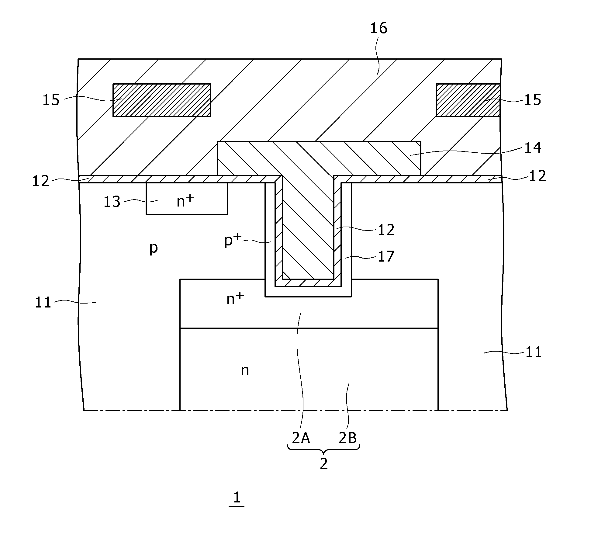
[0035]FIG. 1 is a schematic sectional view showing a pixel portion of a solid-state image sensing device illustrated as a semiconductor device according to a first embodiment of the invention. This embodiment is the case wherein the invention is applied to a CMOS solid-state image sensing device (CMOS image sensor).

[0036]As shown in FIG. 1, a solid-state image sensing device 1 is formed with a transfer transistor made of a vertical NMOS transistor.

[0037]It will be noted that at a section not shown, there are formed transistors (for reset, amplification, selection and the like) each made of a planar NMOS transistor and constituting a pixel.

[0038]At a logic portion, there are formed a planar NMOS transistor and a planar PMOS transistor.

[0039]An n-type impurity region 2 serving as a photodiode of a light-receiving unit is formed at a lower side (back side) of a semiconductor substrate 11 made, for example, of silicon below the vertical NMOS transistor. This n-type impurity region 2 is ...


PUM

PropertyMeasurementUnit
depthaaaaaaaaaa
thicknessaaaaaaaaaa
temperatureaaaaaaaaaa

Abstract

Disclosed herein is a semiconductor device including: a semiconductor substrate; a gate insulating film formed on surfaces of the semiconductor substrate including an internal surface of a hole formed in the semiconductor substrate and formed by radical oxidation or plasma oxidation; and a gate electrode formed as buried in the hole. The gate insulating film and the gate electrode form a vertical MOS.

Description

BACKGROUND OF THE INVENTION[0001]1. Field of the Invention[0002]This invention relates to a semiconductor device having a vertical transistor wherein a gate electrode and a gate insulating film are buried in a semiconductor substrate and a method for manufacturing same. The invention also relates to a solid-state image sensing device having a vertical transistor at a pixel portion.[0003]2. Description of the Related Art[0004]In solid-state image sensing devices, high degrees of integration of circuits have been sought for improving sensitivity and there have been proposed a variety of techniques of keeping the area of a photodiode.[0005]For instance, there is proposed a structure wherein a trench is formed over a photodiode formed at a back side of a silicon substrate and a transfer gate is provided inside the trench thereby forming a vertical transistor (see, for example, Japanese Patent Laid-Open No. 2005-223084, hereinafter referred to as Patent Document 1).[0006]The vertical tra...

Claims


Application Information

Patent Timeline
Patent Type & Authority Applications(United States)
IPC IPC(8): H01L29/78H01L21/336H01L27/146
CPCH01L27/14609H01L27/14645H01L27/14689H01L29/1095H01L27/14612H01L29/4238H01L29/66734H01L29/7813H01L29/4236
Inventor MANDA, SHUJI
Owner SONY CORP
Why Eureka
Try Eureka