

Light emitting apparatus and method for producing the same
a technology of light emitting apparatus and light source, which is applied in the direction of electrical apparatus, semiconductor/solid-state device manufacturing, and semiconductor devices. it can solve the problems of color difference, color unevenness, and difficulty in controlling the outgoing direction of the transverse light component of each unit light source, so as to suppress the loss of the entire luminous flux amount, improve the luminance on the light emission surface, and suppress the appearance of color unevenness
- Summary
- Abstract
- Description
- Claims
- Application Information
AI Technical Summary
Benefits of technology
Problems solved by technology
Method used
Image

Examples
embodiment 1
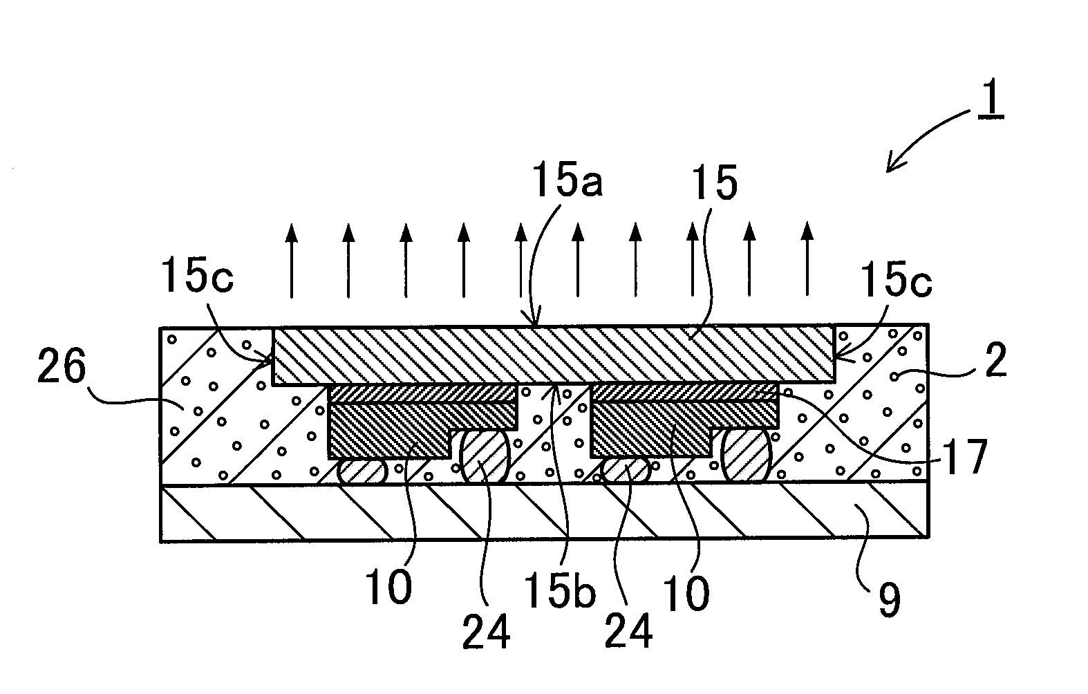
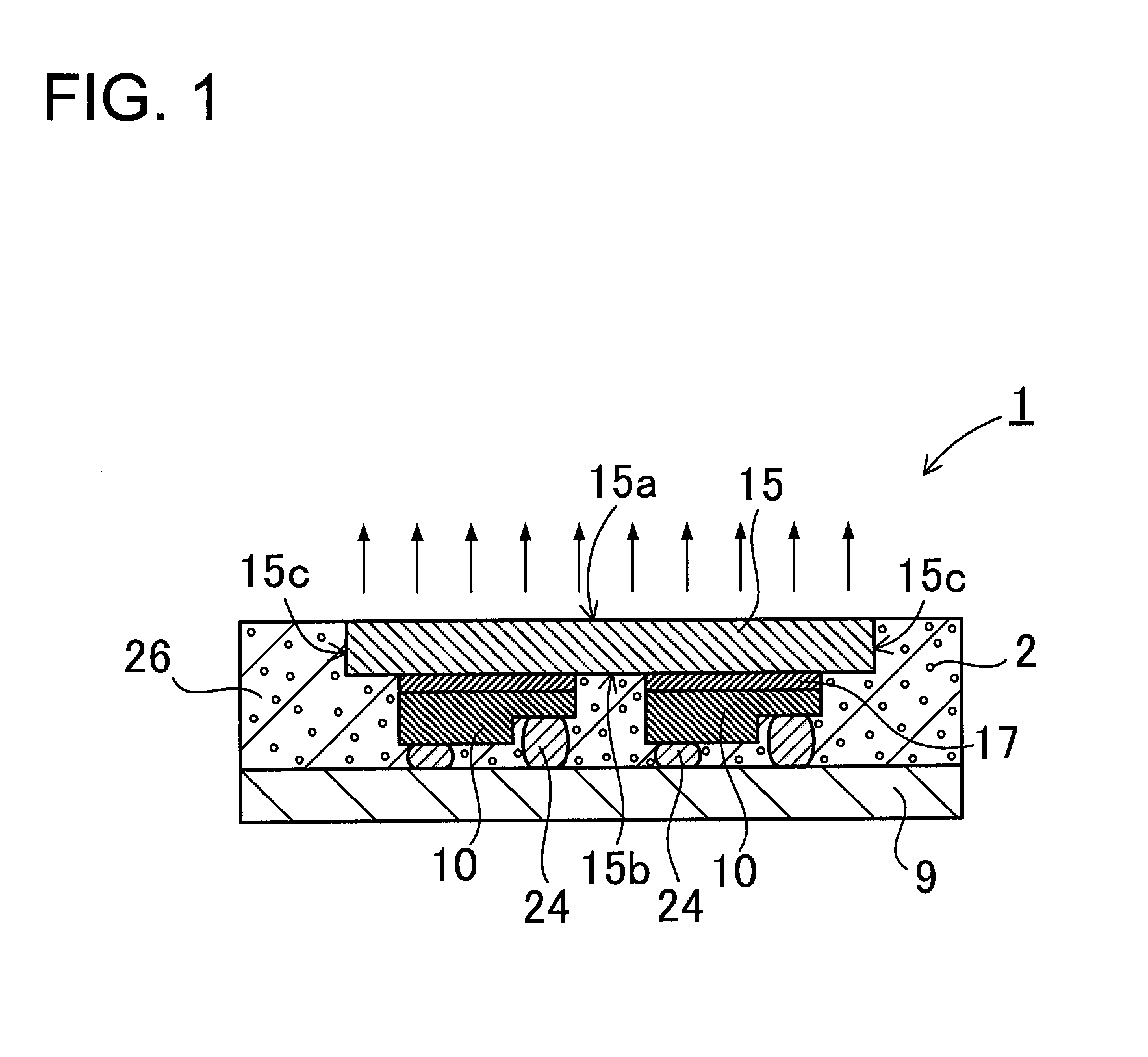
[0038]FIG. 1 is a cross-sectional view schematically showing a light emitting apparatus 1 according to an embodiment 1 of the present invention. The light emitting apparatus 1 according to the example shown in FIG. 1 is principally configured as follows. The light emitting apparatus principally includes light emitting device 10, a light transparent member 15 that allows light emitted from the light emitting device 10 to pass through, and a covering member 26 that partially covers the light transparent member 15. The light emitting device 10 are mounted on a wiring substrate 9 by electrically conductive members 24. The light transparent member 15 is located on the upper side of the light emitting device 10, and optically connected to the light emitting device 10. The light transparent member 15 has a light receiving surface 15b that receives light from the light emitting device 10, and a light emission surface 15a that serves as a plane for emitting the received light and composing t...
embodiment 2
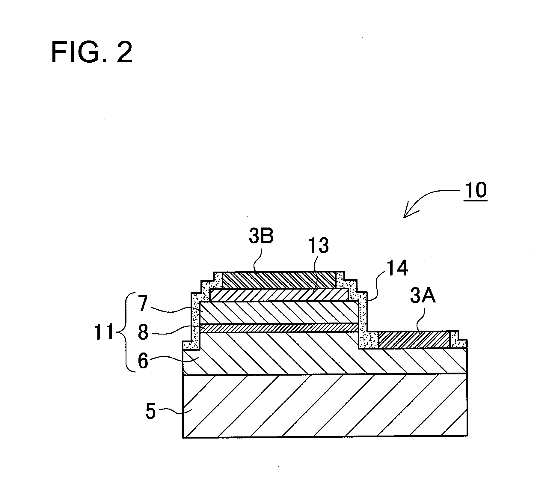
[0099]In an embodiment 2, the light emitting devices 10 are arranged relative to the light transparent member 15 in another exemplary arrangement. FIG. 4 is a schematic cross sectional view showing a light emitting apparatus 20 according to the embodiment 2. In the light emitting apparatus 20 shown in FIG. 4, the side surfaces 15c of the light transparent member 15 are substantially coplanar with the end surfaces 33 of the light emitting devices 10, in other words, the side surfaces of the light transparent member 15 and the light emitting device 10 are substantially coplanar with each other. This arrangement can prevent that color unevenness is likely to occur in a part where the light transparent member protrudes relative to the device in the foregoing embodiment 1, i.e., outer peripheral parts of the light transparent member, due to an insufficient amount of light from the light emitting device. Here, “substantially coplanar” in this specification refers to approximately coplanar...
embodiment 3
[0100]FIG. 5 shows a schematic cross-sectional view showing a light emitting apparatus 30 according to an embodiment 3. In the light emitting apparatus 30 shown in FIG. 5, the light transparent member 15 is laminated on parts of the light emitting devices 10, in other words, the side surface 15c of the light transparent member 15 is located inside the end surface 33 of the light emitting device 10.
[0101]In arrangements shown in FIG. 1 (embodiment 2), FIG. 4 (embodiment 3), and FIG. 5 (this embodiment), the periphery of the light emission surface 15a is covered by the sealing member 26 in a plan view from the light outgoing side. Accordingly, light is not emitted from the outside areas of the sealing member 26 containing the light reflective material 2. In other words, the light emission area of the light emitting apparatus substantially depends on the light emission surface 15a of the light transparent member 15. For this reason, in the arrangement according to the embodiment 1 show...
PUM
 Abstract
Description
Claims
Application Information