Graphene wafer, method for manufacturing the graphene wafer, method for releasing a graphene layer, and method for manufacturing a graphene device

a graphene wafer and graphene technology, applied in the field of graphene wafers, can solve the problems of difficult to obtain graphene sheets having a large area, difficult to transfer epitaxial graphene layers in their entirety onto another substrate, and difficult to obtain epitaxial graphene layers, etc., to achieve good repeatability

Inactive Publication Date: 2010-12-23
OKI DATA CORP
View PDF4 Cites 60 Cited by
  • Summary
  • Abstract
  • Description
  • Claims
  • Application Information

AI Technical Summary

Benefits of technology

[0010]An object of the invention is to provide a graphene wafer, a method for manufacturing a graphene wafer, a method for releasing a graphene laye

Problems solved by technology

Thus, a graphene sheet having a large area is difficult to obtain, which is an obstacle to the process for manufacturing integrated devices.
An epitaxial graphene layer formed on an SiC substrate has a crystal surface which is flat at the atomic level and is chemically firmly bound, so that

Method used


Image

  • Graphene wafer, method for manufacturing the graphene wafer, method for releasing a graphene layer, and method for manufacturing a graphene device
  • Graphene wafer, method for manufacturing the graphene wafer, method for releasing a graphene layer, and method for manufacturing a graphene device
  • Graphene wafer, method for manufacturing the graphene wafer, method for releasing a graphene layer, and method for manufacturing a graphene device

Examples


first embodiment

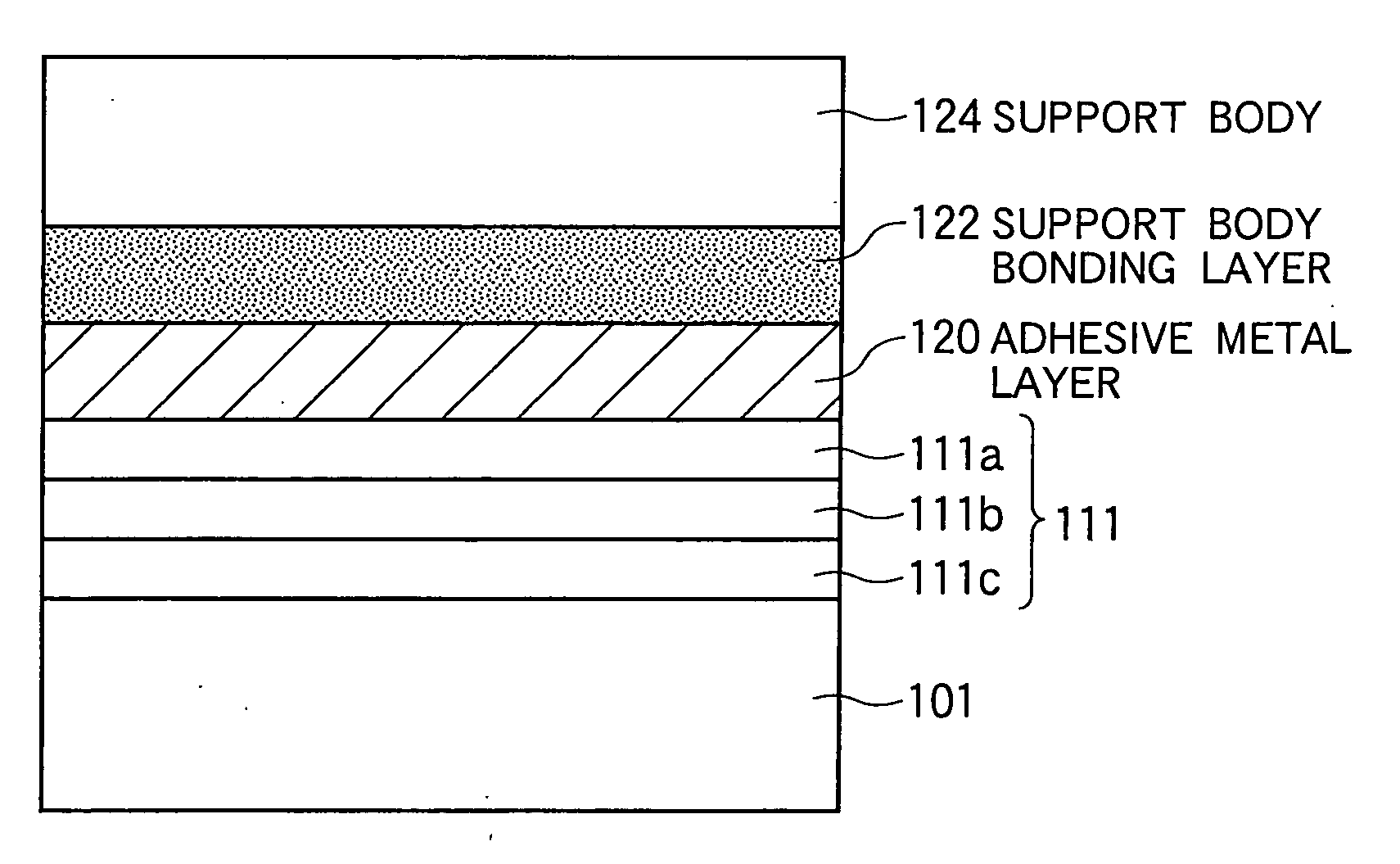
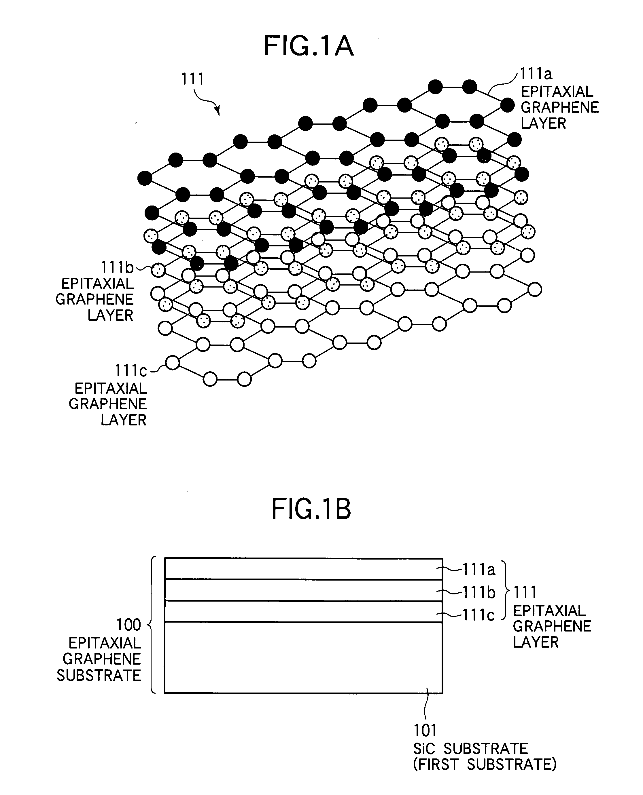
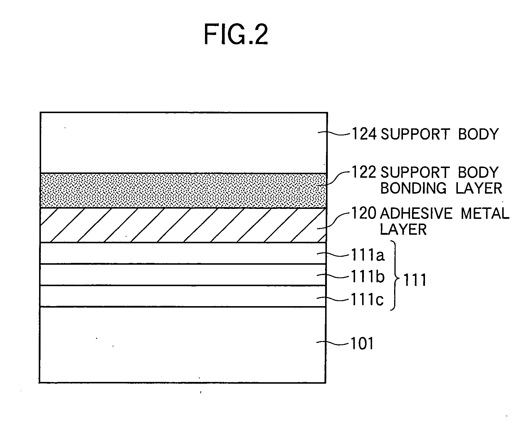
[0066]A first embodiment will be described with reference to FIGS. 1A, 1B, 2, 3A, 3B, 4A, 4B, 5A, 5B, 6, 7A, and 7B. FIGS. 1A and 1B illustrate an epitaxial graphene substrate 100. The epitaxial graphene substrate 100 includes an SiC substrate 101 and an epitaxial graphene layer 111.

[0067]The configuration of the epitaxial graphene layer 111 will be described with reference to FIG. 1A. The epitaxial graphene layer 111 is a flat monolayer of carbon atoms C (solid circles, polka dot pattern circles, and white circles in FIG. 1A) tightly packed into a two-dimensional (2D) honeycomb lattice or a multilayer structure of sheets of the flat monolayer. FIG. 1A is a conceptual representation of a three-layer structure of an epitaxial graphene layer 111a (solid circle), an epitaxial graphene layer 111b (polka dot pattern circle), and an epitaxial graphene layer 111c (white circle). An SiC substrate 101 is subjected to high temperature hydrogen etching and high temperature heat treatment in va...

second embodiment

[0107]The first embodiment is directed to manufacturing a single large-area graphene wafer in which the large-area graphene layer 111a is bonded to the surface of the second substrate 130 or the surface of the bonding layer 132 formed on the second substrate 130. In contrast, a second embodiment is directed to bonding a pre-patterned graphene layer onto a substrate. The second embodiment will be described with respect to FIGS. 8 to 10.

[0108]FIG. 8A is a top view illustrating a graphene pattern.

[0109]FIG. 8B is a cross sectional view illustrating a process for releasing a graphene.

[0110]Referring to FIG. 8A, a graphene layer 111 (not shown) is formed on the surface of an SiC substrate 101 (first substrate) and is patterned by photolithography and then dry-etching using O2 plasma, thereby forming a graphene pattern 210. The graphene pattern 210 in a line pattern shown in FIG. 8A is exemplary and the graphene pattern 210 having any shape is possible.

[0111]Referring to FIG. 8B, the grap...

third embodiment

[0125]A third embodiment is directed to a method of manufacturing a graphene device using a large-area graphene wafer described in the first embodiment. The third embodiment will be described with reference to FIGS. 11-13.

[0126]In the description below, a graphene thin film transistor (TFT) will be used as an exemplary graphene device based on a large-area graphene wafer.

[0127]FIG. 11A illustrates a graphene wafer 300 having a large-area graphene layer formed thereon. The graphene wafer 300 includes an SiO2 film 302 as a bonding layer formed on an n+-SiC substrate 301 and a graphene layer 310 bonded by intermolecular force onto the surface of the SiO2 film 302. The SiO2 film 302 may take the form of a thermally-oxidized film.

[0128]FIG. 11B is a cross-sectional view of the graphene wafer and FIG. 11C is a top view of a graphene wafer. Referring to FIG. 11B and FIG. 11C, a step of photolithography and a step of dry-etching using O2 plasma are performed to pattern the graphene layer 31...


PUM

PropertyMeasurementUnit
Forceaaaaaaaaaa
Structureaaaaaaaaaa
Shapeaaaaaaaaaa

Abstract

A method is used for releasing a graphene layer from a substrate. A graphene layer is first formed on a surface of a first substrate. A metal layer is then formed on a surface of the graphene layer. A pulling force is then applied to the metal layer to detach the graphene layer from the first substrate. The released graphene layer is bonded by intermolecular force onto a surface of a second substrate separate from the first substrate or onto a surface of a bonding layer formed on the surface of the second substrate. The metal layer is then removed, by for example, etching.

Description

BACKGROUND OF THE INVENTION[0001]1. Field of the Invention[0002]The present invention relates a graphene wafer, a method for manufacturing a graphene wafer, a method for releasing a graphene layer from a substrate, and a method for manufacturing a graphene device.[0003]2. Description of the Related Art[0004]The Scotch tape method as a transfer technique of graphene was reported in 2004 by A. Gaim et al. of Manchester University in United Kingdom. They succeeded in mechanically transferring a single layer of graphene onto an SiO2 / Si substrate from a highly oriented pyrolytic graphite (HOPG).[0005]Graphene is a massless Dirac fermion material having a unique band structure and provides almost all useful electrical properties of carbon nanotubes having a structure of a tube including ballistic conduction, which will attracts engineer interest. Graphene is a new material having a sheet-like structure as opposed to carbon nanotubes (CNT), and therefore lends itself to micromachining used...

Claims


Application Information

Patent Timeline
IPC IPC(8): B32B3/26C01B31/04B32B38/10
CPCY10T428/30H01L21/02664H01L21/02527Y10T156/1168H01L21/02378Y10T428/24479H01L21/2007
Inventor OGIHARA, MITSUHIKOSAGIMORI, TOMOHIKOSAKUTA, MASAAKIHASHIMOTO, AKIHIROTANAKA, SATORU
Owner OKI DATA CORP
Why Eureka
Try Eureka