
Manufacturing method of semiconductor photonic device substrate

a manufacturing method and photonic device technology, applied in semiconductor/solid-state device testing/measurement, mechanical measuring arrangements, instruments, etc., can solve the problems of difficult to measure the thickness of the semiconductor photonic device substrate in a non-destructive manner, the quality of the fabricated photonic device substrate does not meet the control standard, and the thickness of the film is difficult to achieve. , the effect of reducing the number of operation steps and reducing the number of gas materials

Inactive Publication Date: 2011-01-06
SUMITOMO CHEM CO LTD
View PDF2 Cites 0 Cited by
  • Summary
  • Abstract
  • Description
  • Claims
  • Application Information

AI Technical Summary

Benefits of technology

[0018]An object of the present invention is to reduce this large number of items of the growth rate preinspection in the preinspection operation.
[0035]Furthermore, when the parameter of the inter-layer growth rate model using various types of films as the input is to be obtained, the PLS regression analysis is used. Therefore, the parameter can be calculated with a smaller number of actual result samples than the number of inputs while ensuring the estimation accuracy based on the correlation in growth rate between respective films. More specifically, the inter-layer growth rate model and its parameter can be determined with a smaller number of actual result samples than that of the case using the multiple regression analysis in which actual result samples more than the number of inputs are required, and the growth rate preinspection operation can be reduced early.

Problems solved by technology

When repeating the process several tens of times, reactants are attached inside the chamber, so that the quality of the fabricated photonic device substrates does not satisfy the control standard.
In the semiconductor photonic device substrate, crystal growth of a large number of layers is successively performed, and since the multiple layers are provided and they have significantly different thicknesses, it is difficult to measure the thickness of the semiconductor photonic device substrate in a non-destructive manner.
In this measurement method, however, the X-ray reflectometry apparatus is required, and the number of types of the stacked films (two types of GaAs and AlGaAs in the embodiment) and the film thickness (20 to 40 nm in the embodiment) are assumed to have a physical limit due to the interference in the reflectometry.
Due to these problems, the method of Patent Document 2 is not suitable for the film thickness measurement of the multiple-material / multiple-layer stacked films having different thicknesses.

Method used


Image

  • Manufacturing method of semiconductor photonic device substrate
  • Manufacturing method of semiconductor photonic device substrate
  • Manufacturing method of semiconductor photonic device substrate

Examples


first embodiment

[0060]The first embodiment will be described with reference to FIGS. 6, 7 and 8.

[0061]First, the feasibility of the estimation of a growth rate of a film corresponding to a certain layer based on a growth rate of a film corresponding to another layer will be described.

[0062]FIG. 6 shows the growth rate trend by maintenance in an MOCVD equipment A. An x axis represents the maintenance [number of times (about once per month)], and a y axis represents the growth rate. A total of six growth rate preinspection results after the maintenances are shown. The growth rates of the films corresponding to the layers other than the DBR layer 2 change with the same trend of fall, rise, large rise, large fall and rise from the first growth rate to the sixth growth rate. In other words, the changing patterns of each maintenance have a correlation with each other.

[0063]So, FIG. 7 shows a correlation matrix using the six samples about the growth rates of all layers of the preinspection. It is possible...

second embodiment

[0068]The second embodiment will be described with reference to FIG. 9.

[0069]The method of estimating the growth rate based on the inter-layer growth rate model by use of the growth rate preinspection results for a part of the films corresponding to the layers of the semiconductor photonic device substrate and then obtaining the growth time of all films corresponding to the layers is shown by the flowchart in FIG. 9.

[0070]The target of growth rate estimation will be described with using an example of the estimation based on the single-input single-output inter-layer growth rate model in which the growth rate of the current diffusion layer (current correction layer) is estimated from only the growth rate preinspection result of the temperature check (growth rate check) (hereinafter, referred to as estimation target example 1) and an example of the estimation based on the multiple-input single-output inter-layer growth rate model in which the growth rate of the active layer (barrier l...

third embodiment

[0082]The third embodiment will be described with reference to FIG. 10.

[0083]The method of obtaining the inter-layer growth rate model, in which the error of the growth rate estimated value to the actual result value is minimized, from the candidates of various inter-layer growth rate models by using the past growth rate actual result values in each growth rate preinspection performed after the maintenance will be described.

[0084]For the estimation of the growth rate, the parameter of the inter-layer growth rate model is obtained by using the growth rate actual result values of the films to be an input and an output. And so, the method of calculating the parameter of the inter-layer growth rate model will be first described.

[0085]In the case of the single-input single-output inter-layer growth rate model, in particular, in the case where the model is defined by the proportional relation, the parameter can be estimated if there are one or more actual result samples of the growth rate...


PUM

PropertyMeasurementUnit
thicknessaaaaaaaaaa
compositionaaaaaaaaaa
thicknessaaaaaaaaaa

Abstract

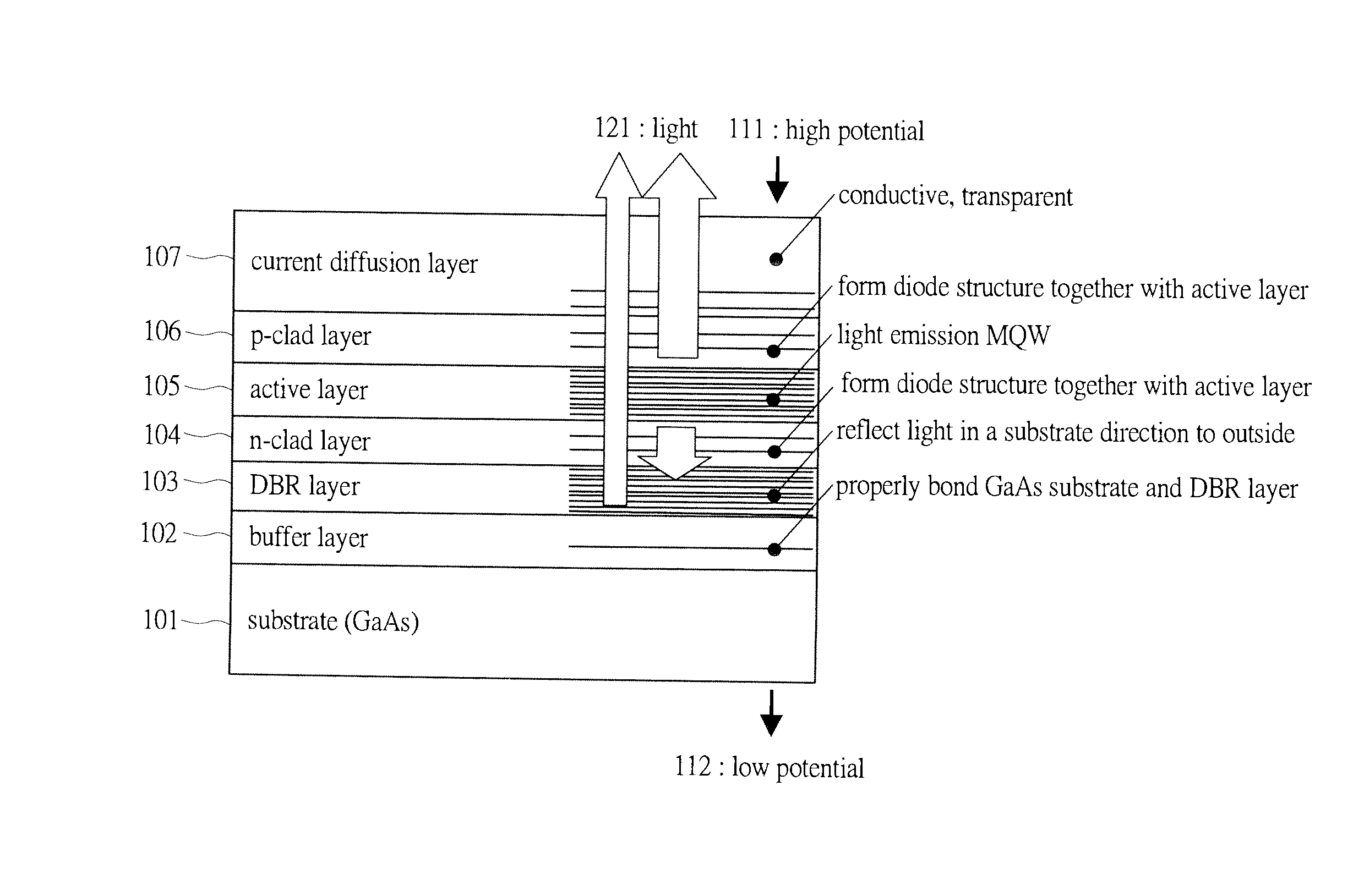
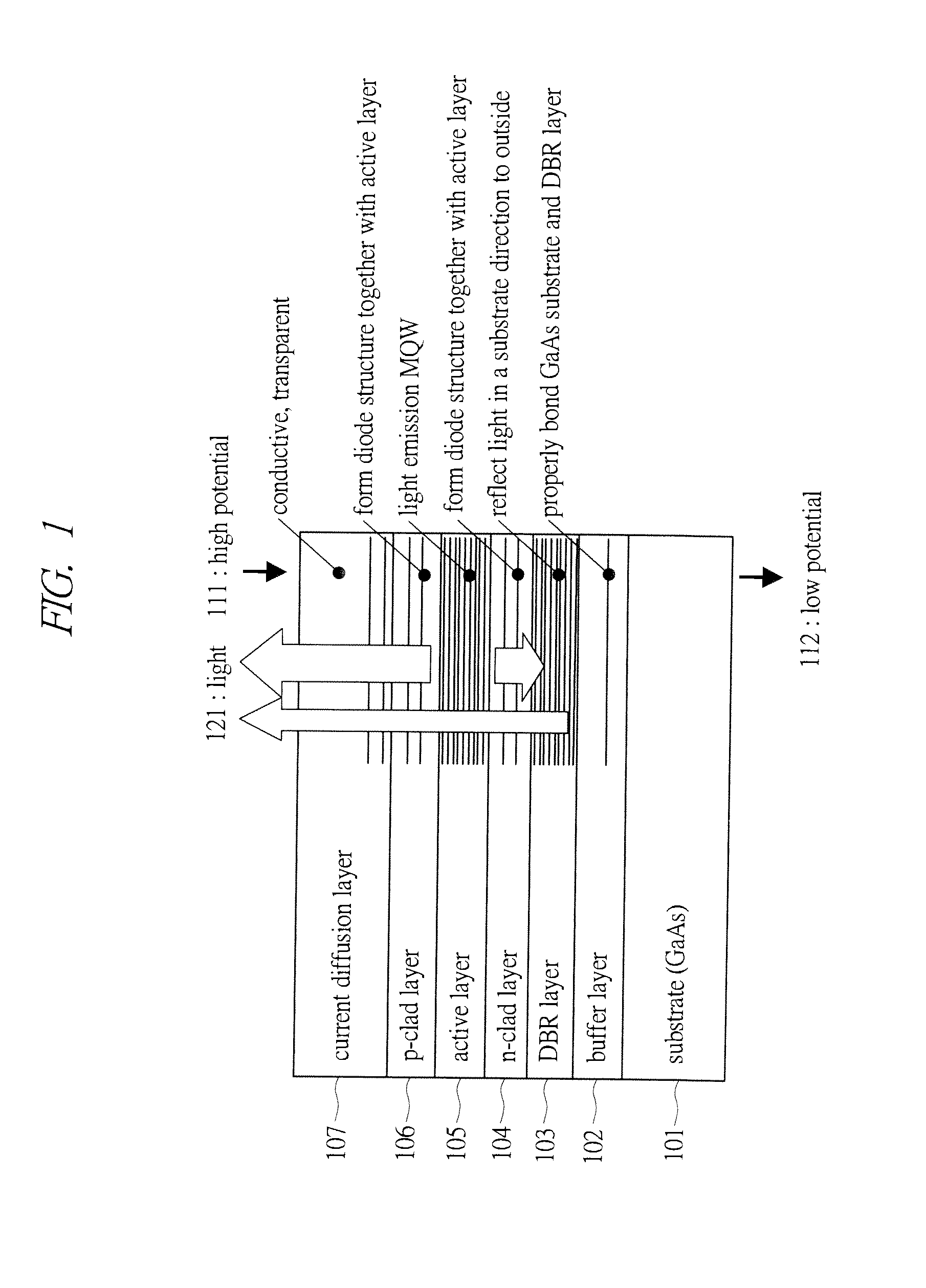
In a manufacturing method of a semiconductor photonic device substrate, before multi-layer films different in material composition are successively and gradually crystal-grown in one chamber, an inter-layer growth rate model showing a relation in growth rate between each layer is defined, a growth rate of a film corresponding to at least one or more layers is obtained by actual crystal growth using an individual substrate, a growth rate of a film corresponding to other layers is estimated from the obtained growth rate by the inter-layer growth rate model, and a growth time is determined in accordance with a film thickness of each layer of the semiconductor photonic device substrate based on the actually obtained growth rate and the estimated growth rate. These steps are carried out by using a computer system connected to an MOCVD equipment, and then, a crystal growth of the semiconductor photonic device substrate is performed.

Description

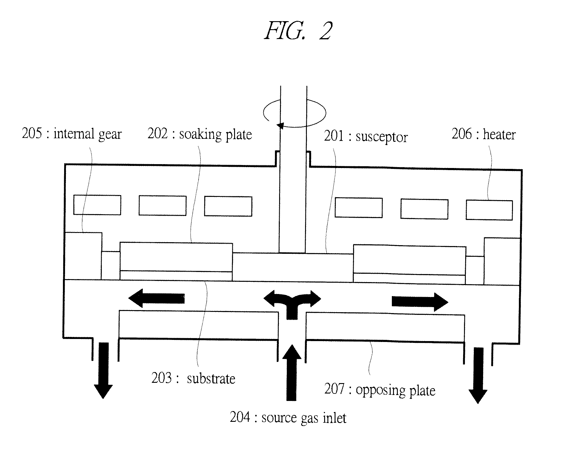
CROSS-REFERENCE TO RELATED APPLICATION[0001]The present application claims priority from Japanese Patent Application No. 2009-159182 filed on Jul. 3, 2009, the content of which is hereby incorporated by reference into this application.TECHNICAL FIELD OF THE INVENTION[0002]The present invention relates to a method for omitting a growth rate preinspection operation by estimating a growth rate of crystal growth in the manufacture of a semiconductor photonic device such as an LED (Light Emitting Diode) in which multi-layer thin films different in composition need to be crystal-grown on a substrate (wafer) by using an MOCVD (Metal Organic Chemical Vapor Deposition, also referred to as MOVPE (Metal Organic Vapor Phase Epitaxy) equipment. After maintenance, only apart of the films with certain compositions are crystal-grown by using an individual substrate to perform the preinspection of the growth rate, and then, the growth rates of the films with other compositions are estimated based on...

Claims


Application Information

Patent Timeline
Patent Type & Authority Applications(United States)
IPC IPC(8): H01L21/20
CPCC23C16/56H01L21/02395H01L33/46H01L33/007H01L21/02543
Inventor MORISAWA, TOSHIHIROTANI, TAKEHIKONAGAI, HISATAKAFURUYA, TAKASHI
Owner SUMITOMO CHEM CO LTD
Learn More