Clock signal amplifier circuit

Inactive Publication Date: 2011-01-20
PANASONIC CORP
View PDF9 Cites 3 Cited by
  • Summary
  • Abstract
  • Description
  • Claims
  • Application Information

AI Technical Summary

Benefits of technology

With the above configuration, when the logic threshold potential of the inverter or the logic circuit deviates from an ideal value due to fabrication variations in the CMOS process, the potential at the connection node of the two res

Problems solved by technology

Although high-speed startup can be achieved, the conventional clock signal amplifier circuit described above, having a number of additional circuits, inevitably increases the development cost and the production cost.
Moreover, w

Method used


Image

  • Clock signal amplifier circuit
  • Clock signal amplifier circuit
  • Clock signal amplifier circuit

Examples


first embodiment

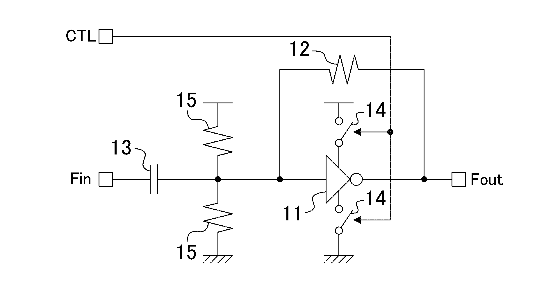
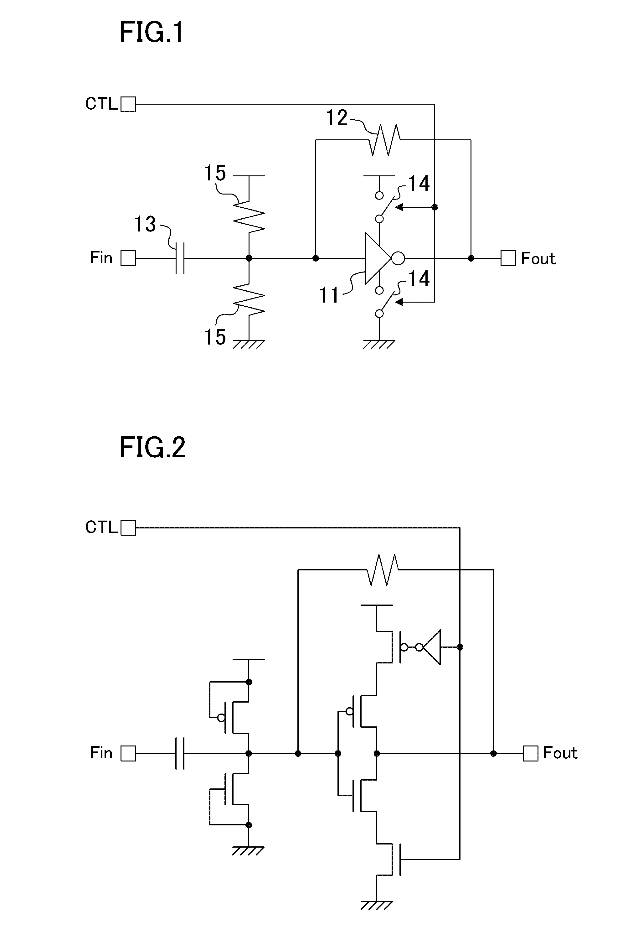
FIG. 1 shows a configuration of a clock signal amplifier circuit of the first embodiment. In the clock signal amplifier circuit of this embodiment, a feedback resistor 12 is connected between the input and output of an inverter 11. The inverter 11 amplifies the AC component of a small-amplitude clock signal Fin input via a coupling capacitor 13 and outputs a clock signal Fout.

Switches 14 are respectively provided on supply paths of the power supply potential and the ground potential to the inverter 11. These switches 14 perform the same open / close operation according to a control signal CTL. For example, the switches 14 are conducting when the control signal CTL is high, and are not conducting when the control signal CTL is low.

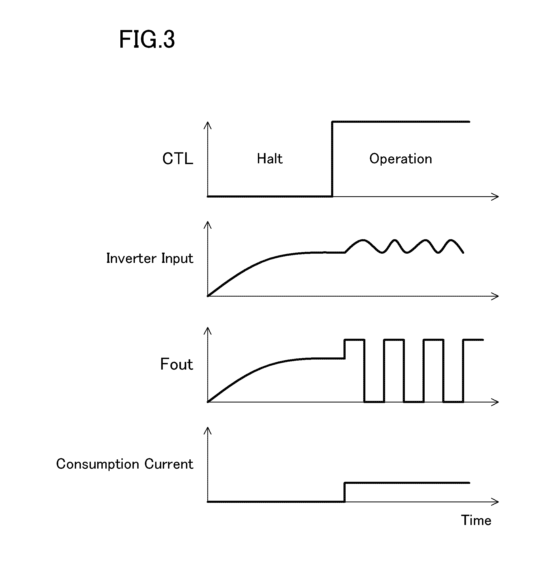
As the control signal CTL, a hardware reset signal for the entire system including the clock signal amplifier circuit can be used. In other words, the clock signal amplifier circuit can be controlled so that it is halted when the entire system is being reset ...

second embodiment

FIG. 6 shows a configuration of a clock signal amplifier circuit of the second embodiment. In the clock signal amplifier circuit of this embodiment, a feedback resistor 12 and a switch 14 are connected between the output and one input of a 2-input NAND element 16. The switch 14 performs open / close operation according to a high-active control signal CTL. In other words, the switch 14 is conducting when the control signal CTL is high, and not conducting when the control signal CTL is low. The control signal CTL is also input into the other input of the NAND element 16. The NAND element 16 amplifies the AC component of a small-amplitude clock signal Fin input via a coupling capacitor 13 and outputs a clock signal Fout. The coupling capacitor 13 and two resistors 15 are the same as those described above.

FIG. 7 shows a specific circuit configuration of the clock signal amplifier circuit of FIG. 6, in which the reference characters are omitted. As shown in FIG. 7, the two resistors 15 can...

third embodiment

FIG. 9 shows a configuration of a clock signal amplifier circuit of the third embodiment. The clock signal amplifier circuit of this embodiment includes a resistor circuit 17 connected in parallel with the feedback resistor 12 in addition to the configuration of the clock signal amplifier circuit of the first embodiment. Only points different from the first embodiment will be described hereinafter.

The resistor circuit 17 includes: an integrator circuit 171 that integrates the control signal CTL; and a transistor 172 that is connected in parallel with the feedback resistor 12 and to the gate of which the output of the integrator circuit 171 is applied. In other words, in the resistor circuit 17, the resistance value increases with the CR time constant of the integrator circuit 171 after transition of the control signal CTL from low to high. In this embodiment, the transistor 172 is of p-type because the control signal CTL is assumed to be high-active. When the control signal CTL is l...


PUM


Abstract

A clock signal amplifier circuit includes: an inverter; a coupling capacitor connected to the input of the inverter; two resistors connected in series between the power supply potential and the ground potential, a connection node of the two resistors being connected to the input of the inverter; a feedback resistor provided between the input and output of the inverter; and two switches configured to perform a same open/close operation according to a control signal, the two switches being provided on any two of a supply path of the power supply potential to the inverter, a supply path of the ground potential to the inverter, and a feedback path of the inverter via the feedback resistor.

Description

BACKGROUNDThe present disclosure relates to a clock signal amplifier circuit that amplifies an input small-amplitude clock signal to a voltage large enough to be usable in digital circuits.In semiconductor integrated circuits, a clock signal is necessary for computing digital circuits. In general, a clock signal is generated by a quartz oscillator or a clock generation IC placed outside a semiconductor integrated circuit and then input into the semiconductor integrated circuit in many cases. When the amplitude of the clock signal input into the semiconductor integrated circuit is the same as the power supply amplitude of the semiconductor integrated circuit, the input clock signal can be used as it is. However, if the former is smaller than the latter, the clock signal may possibly disappear without being taken into the semiconductor integrated circuit. For this reason, a clock signal amplifier circuit is required for amplifying a small-amplitude clock signal up to the level of the ...

Claims


Application Information

Patent Timeline
IPC IPC(8): H03L5/00
CPCH03K19/018571H03K19/017545
Inventor KINOSHITA, MASAYOSHISOGAWA, KAZUAKIYAMADA, YUJI
Owner PANASONIC CORP
Why Eureka
Try Eureka