Method for manufacturing semiconductor device, and semiconductor manufacturing apparatus used in said method

a manufacturing apparatus and semiconductor technology, applied in the direction of solid-state diffusion coating, chemical vapor deposition coating, coating, etc., can solve the problems of thermal alteration (a chemical reaction, chemically-altered flux is not easily dissolved with an organic solvent), and achieve the effect of higher yield in manufacturing the semiconductor devi

Inactive Publication Date: 2011-01-20
RENESAS ELECTRONICS CORP
View PDF23 Cites 5 Cited by
  • Summary
  • Abstract
  • Description
  • Claims
  • Application Information

AI Technical Summary

Benefits of technology

[0013]According to the present invention, the reactive oxygen gas is supplied after the solder bump is formed by melting the solder. Therefore, the flux chemically altered through a heating treatment for melting the solder can be removed from the solder bump. Accordingly, a solder bump of an interconnect substrate and the solder bump of the semiconductor element can be properly connected.
[0014]According to the present invention, a solder bump of an interconnect substrate and the solder bump of the semiconductor element can be properly connected. Thus, yield in manufacturing the semiconductor device can be made higher.

Problems solved by technology

However, it has become apparent from findings by the inventor that flux has following problems.
Flux might cause a thermal alteration (a chemical reaction) during a heat treatment for melting solder.
The chemically-altered flux is not easily dissolved with an organic solvent.
When a semiconductor element formed on a substrate with remaining flux on surfaces of solder bumps is mounted on an interconnect substrate, electric contact failures are caused between the solder bumps of the interconnect substrate and the solder bumps of the semiconductor element.
As a result, yield in manufacturing the semiconductor device is lowered.
By any of the conventional techniques disclosed in Japanese Laid-Open Patent Publication Nos. 2004-6818, 2007-266054, and 2008-41980, however, the chemically-altered flux cannot be removed.

Method used


Image

  • Method for manufacturing semiconductor device, and semiconductor manufacturing apparatus used in said method
  • Method for manufacturing semiconductor device, and semiconductor manufacturing apparatus used in said method
  • Method for manufacturing semiconductor device, and semiconductor manufacturing apparatus used in said method

Examples


first modification

[First Modification]

[0043]For example, although the solder paste 13 is applied onto the electrode pad 11 in the above embodiment, a solder bump may also be formed by performing plating on an electrode pad in the present invention.

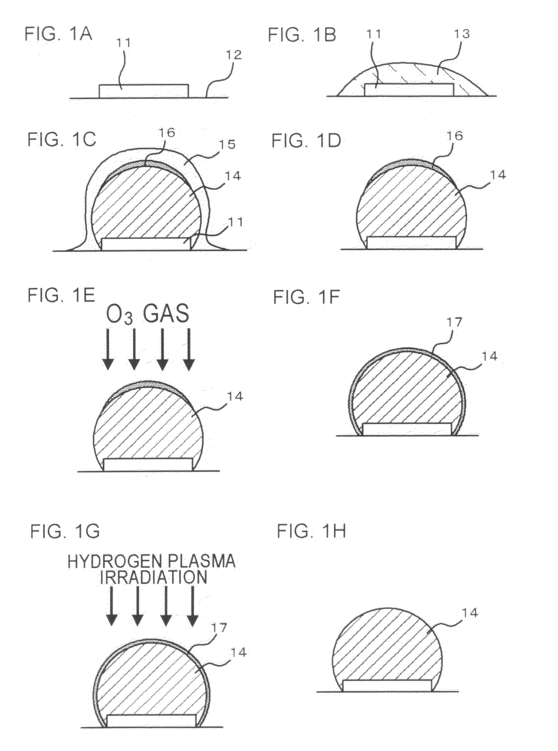
[0044]FIGS. 3A through 3I are drawings for explaining this first modification. First, plating is performed on a substrate 32 having an electrode pad 31 formed thereon (FIG. 3A) with the use of a patterning film such as a photoresist. As a result, a solder-plate film 33 is formed on the electrode pad 31 (FIG. 3B).

[0045]After the photoresist as the patterning film is removed, flux 35 is applied so as to cover the electrode pad 31 and the solder-plate film 33 (FIG. 3C).

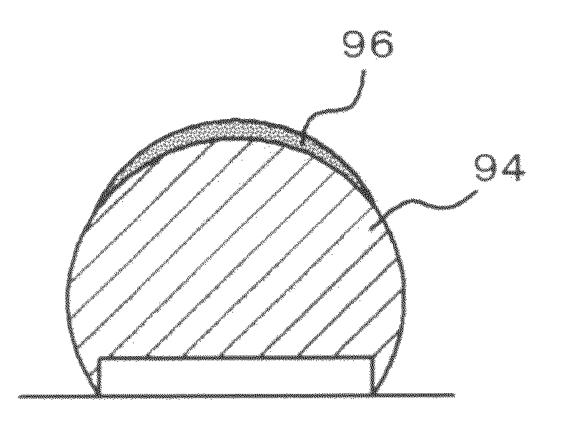
[0046]A heating treatment is then performed to melt the solder-plate film 33 and form a solder bump 34. At this point, part of the flux 35 is chemically altered, and the chemically-altered flux 36 remains on the surface of the solder bump 34 (FIG. 3D).

[0047]The flux 35 is then removed with the u...

second modification

[Second Modification]

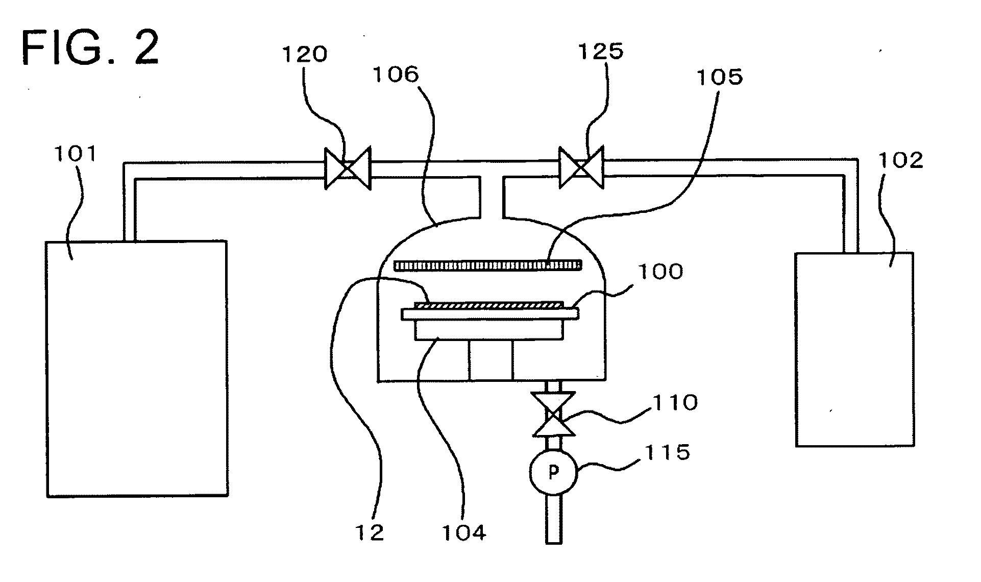
[0051]Although the flux 35 is used in the above described modification, the flux 35 may not be used. Referring now to FIG. 4A through 4C, a second modification is described in detail. In FIGS. 4A through 4C, the processes to form the solder-plate film 33 on the substrate 32 having the electrode pad 31 formed thereon (FIG. 4A) by performing plating with the use of a patterning film such as a photoresist are the same as those of the above modification (FIG. 4B). In FIG. 4C, the solder-plate film 33 is heated with concurrently irradiated with hydrogen plasma to form the solder bump 34. Since the flux 35 is not used in this second modification, an O3 gas exposure is unnecessary and the number of manufacturing processes can be reduced. Furthermore, since the chemically-altered flux 36 that is hard to remove is not generated, the solder bumps of the interconnect substrate and the solder bumps of the semiconductor substrate can be properly connected.

[0052]Hereinafter, ...


PUM

PropertyMeasurementUnit
melting temperatureaaaaaaaaaa
exposure timeaaaaaaaaaa
timeaaaaaaaaaa

Abstract

This method includes an electrode pad forming process for forming an electrode pad on a substrate, a solder bump forming process for forming a solder bump on the electrode pad, at least part of the surface of the solder bump being covered with a flux, and an oxygen exposure process for supplying an oxygen gas having reactive properties, such as an ozone (O3) gas, to the solder bump.

Description

[0001]This application is based on Japanese patent application No. 2009-166657, the content of which is incorporated hereinto by reference.BACKGROUND[0002]1. Technical Field[0003]The present invention relates to a method for manufacturing a semiconductor device, and a semiconductor manufacturing apparatus used in the method.[0004]2. Related Art[0005]As portable electronic devices have been becoming smaller and achieving higher speeds in recent years, flip-chip mounting technique is now widely used to connect semiconductor chips to interconnect substrates not by wire bonding but with solder bumps. In the flip-chip mounting, interconnect lengths can be made shorter, and higher-speed transmission characteristics can be achieved than in a case where connections are performed by wire bonding. Also, smaller packages can be realized.[0006]As such a method for forming a solder bump, Japanese Laid-Open Patent Publication No. 2004-6818 discloses a method by which a solder paste is applied by ...

Claims


Application Information

Patent Timeline
Patent Type & Authority Applications(United States)
IPC IPC(8): H01L21/60C23C16/458
CPCC23C8/12H01L2924/00013H01L24/11H01L2924/01078H01L2924/01082H01L2924/01005H01L2924/01006H01L2924/01033H01L2924/014H01L2224/1152H01L24/13H01L2224/1132H01L2224/1146H01L2224/1181H01L2224/131H01L2224/742H01L2224/13006C23C8/36H01L2924/00014H01L2224/13099H01L2224/13599H01L2224/05599H01L2224/05099H01L2224/29099H01L2224/29599
Inventor SHIMIZU, YUJI
Owner RENESAS ELECTRONICS CORP
Why Eureka
Try Eureka