Semiconductor device

Inactive Publication Date: 2011-01-27
RENESAS ELECTRONICS CORP
View PDF2 Cites 13 Cited by
  • Summary
  • Abstract
  • Description
  • Claims
  • Application Information

AI Technical Summary

Benefits of technology

[0018]In Japanese Unexamined Patent Application Publication No. 2002-124575, the metallization wirings 201 having different polarities are alternately formed in the top layer thereof. Thus, the design flexibility of the top layer of the metallization wirings 201 is not high. According to the present invention, emergence portions of the capacity electrodes having different po

Problems solved by technology

Therefore, it becomes more difficult to secure an area in which the capacitative elements are inserted.
However, from the viewpoint of workability, it is extremely difficult to miniaturize the parallel flat plate as disclosed in Japanese Unexamined Patent Application Publication No. 2005-136300, along with the advancement in nanofabrication technology.
However, in Japanes

Method used


Image

  • Semiconductor device
  • Semiconductor device
  • Semiconductor device

Examples


first exemplary embodiment

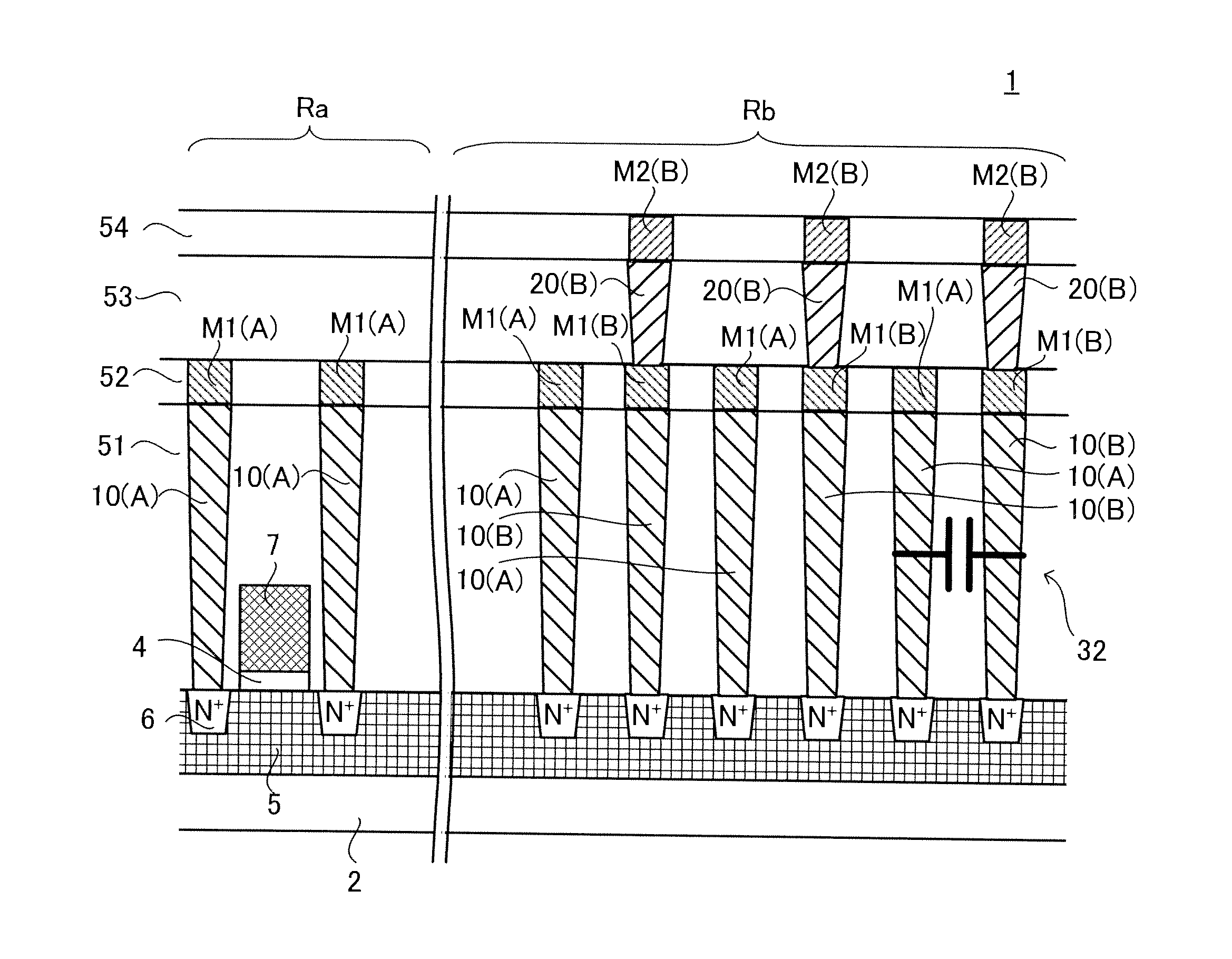
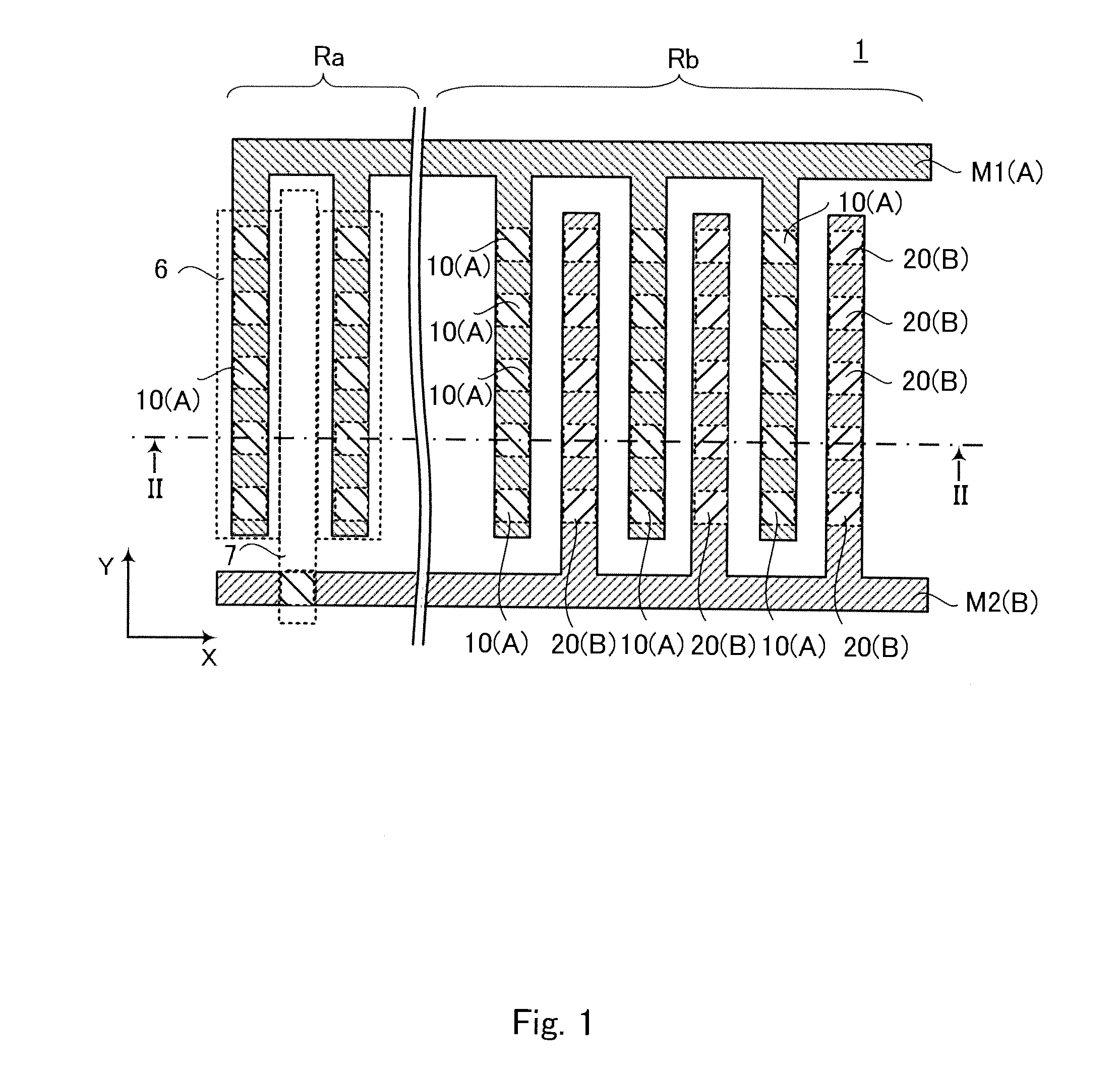
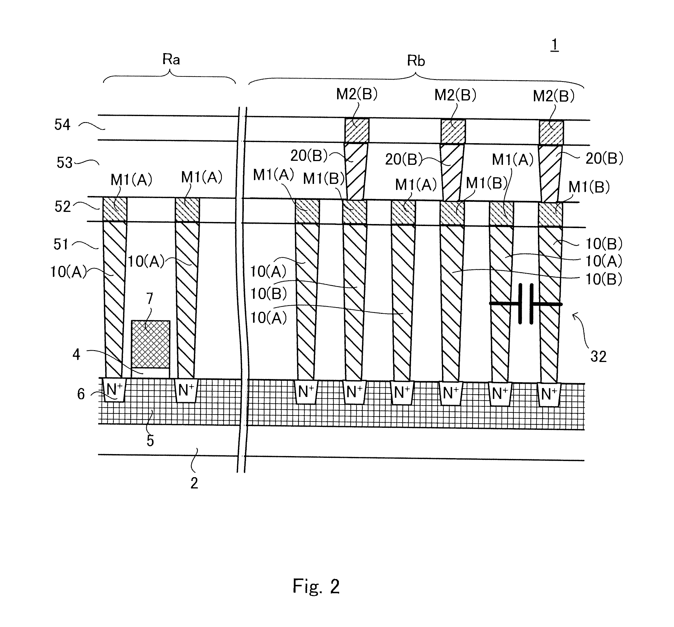
[0041]FIG. 1 is a schematic plane view of a semiconductor device according to a first exemplary embodiment of the present invention. FIG. 2 is a sectional view taken along the line II-II of FIG. 1. In FIG. 1, the positions of contact plugs are indicated by dotted lines for convenience of the explanation thereof.

[0042]A semiconductor device 1 includes a semiconductor substrate 2, active regions 6, a gate insulating film 4, a gate electrode layer 7, side walls (not shown), first layer wirings M1 and second layer wirings M2 functioning as layer wirings, contact plugs to be described later, a first interlayer dielectric 51, a second interlayer dielectric 52, a third interlayer dielectric 53, and a fourth interlayer dielectric 54.

[0043]Note that the term “layer wiring” herein described refers to an electrically conductive layer of the bottom layer in the wirings that are connected at an upper part of the contact plug, and to electrically conductive layers formed above the bottom layer in...

second exemplary embodiment

[0069]Next, a description is given of an example of a semiconductor device which is different from the above-mentioned exemplary embodiment. FIG. 5 shows a schematic sectional view of a semiconductor device 1a according to a second exemplary embodiment of the present invention. The semiconductor device 1a has the logic section Ra, the capacitative element section Rb, and a DRAM (Dynamic Random Access Memory) section Rc. As described earlier, the parasitic capacity between the wirings has been increasing along with the recent advancement in miniaturization of semiconductor devices. Therefore, the parasitic capacity between the contact plugs formed by an advanced process becomes not negligible. Particularly, in the case of a configuration in which contact plugs have a large height, such as a mixed DRAM of a stack type, the influence of the parasitic capacity has become more remarkable. The semiconductor device according to the second exemplary embodiment positively uses the parasitic ...

third exemplary embodiment

[0081]Next, a description is given of an example of a semiconductor device which is different from the first exemplary embodiment. The basic configuration of a semiconductor device 1b according to a third exemplary embodiment of the present invention is similar to that of the first exemplary embodiment, except for the following. That is, in the first exemplary embodiment, the first electrode plugs 10(A) and the second electrode plugs 10(B) have a configuration in which layer wirings (the first layer wirings M1, the second layer wirings M2) and the active regions 6 are connected to each other. Meanwhile, in the third exemplary embodiment, the first electrode plugs and second electrode plugs are disposed between an element isolation region 3 and layer wirings (the first layer wirings M1, the second layer wirings M2).

[0082]FIG. 6 shows a schematic sectional view of the semiconductor device according to the third exemplary embodiment of the present invention. As shown in FIG. 6, first e...


PUM


Abstract

A semiconductor device including: multiple layer wirings which are formed above a semiconductor substrate; multiple first electrode type contact plugs which have a granular shape in plane view, extend in a lower direction from the layer wirings to be connected to the layer wirings on an upper side, and serve as a first electrode; multiple second electrode type contact plugs which have a granular shape in plane view, extend in the lower direction from the layer wirings to be connected to the layer wirings on an upper side, and serve as a second electrode different from the first electrode; and a capacitative element section that fauns a capacity between adjacent ones of the first electrode type contact plugs and second electrode type contact plugs. The layer wirings serving as emergence portions of capacity electrodes of the first and second electrode type contact plugs are formed by different layer wirings.

Description

INCORPORATION BY REFERENCE[0001]This application is based upon and claims the benefit of priority from Japanese patent application No. 2009-170857, filed on Jul. 22, 2009, the disclosure of which is incorporated herein in its entirety by reference.BACKGROUND[0002]1. Field of the Invention[0003]The present invention relates to a semiconductor device, and more particularly, to a semiconductor device including a capacitative element.[0004]2. Description of Related Art[0005]Along with the recent speeding-up of semiconductor devices, more decoupling capacitative elements are required to prevent noise. Meanwhile, the semiconductor devices have been miniaturized. Therefore, it becomes more difficult to secure an area in which the capacitative elements are inserted.[0006]As a method to provide a semiconductor device that suppresses an increase in area thereof and includes a capacitative element having a high capacitance value, Japanese Unexamined Patent Application Publication No. 2005-1363...

Claims


Application Information

Patent Timeline
IPC IPC(8): H01L27/108
CPCH01L23/5223H01L27/0207H01L27/10852H01L27/10894H01L27/10897H01L2924/0002H01L28/87H01L28/91H01L2924/00H10B12/09H10B12/50H10B12/033
Inventor IZUMI, KATSUYAAOGAKI, KAZUTOSHI
Owner RENESAS ELECTRONICS CORP
Why Eureka
Try Eureka