Semiconductor device and method for manufacturing semiconductor device

a semiconductor and semiconductor technology, applied in the field of semiconductor devices, can solve the problems of increased power consumption, signal waveform distortion, signal transmission delay, etc., and achieve the effects of stable electric characteristics, favorable electric characteristics, and high reliability

Active Publication Date: 2011-02-10
SEMICON ENERGY LAB CO LTD
View PDF99 Cites 67 Cited by
  • Summary
  • Abstract
  • Description
  • Claims
  • Application Information

AI Technical Summary

Benefits of technology

[0056]According to an embodiment of the present invention, a thin film transistor having stable electric characteristics can be manufactured and provided. Thus, a semiconductor device which includes highly reliable thin film transistors with favorable electric characteristics can be provided.

Problems solved by technology

This capacitance is also called parasitic capacitance between wirings, and distortion of signal waveforms may occur.
Further, when parasitic capacitance is large, signal transmission may be delayed.
Furthermore, an increase in parasitic capacitance leads to a cross talk phenomenon in which an electric signal leaks between wirings and an increase in power consumption.
In an active matrix display device, particularly when large parasitic capacitance is generated between a signal wiring which supplies an image signal and another wiring or an electrode, display quality may be deteriorated.
Moreover, when miniaturization of the circuit is achieved, a distance between wirings is short, and parasitic capacitance between wirings may increase.

Method used


Image

  • Semiconductor device and method for manufacturing semiconductor device
  • Semiconductor device and method for manufacturing semiconductor device
  • Semiconductor device and method for manufacturing semiconductor device

Examples


embodiment 1

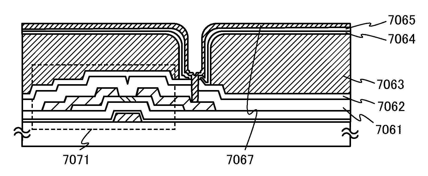
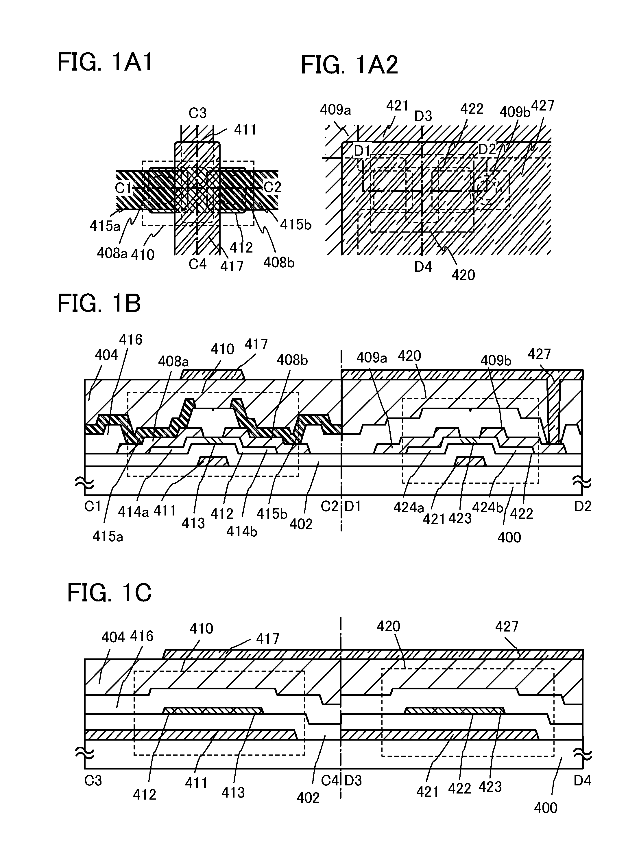
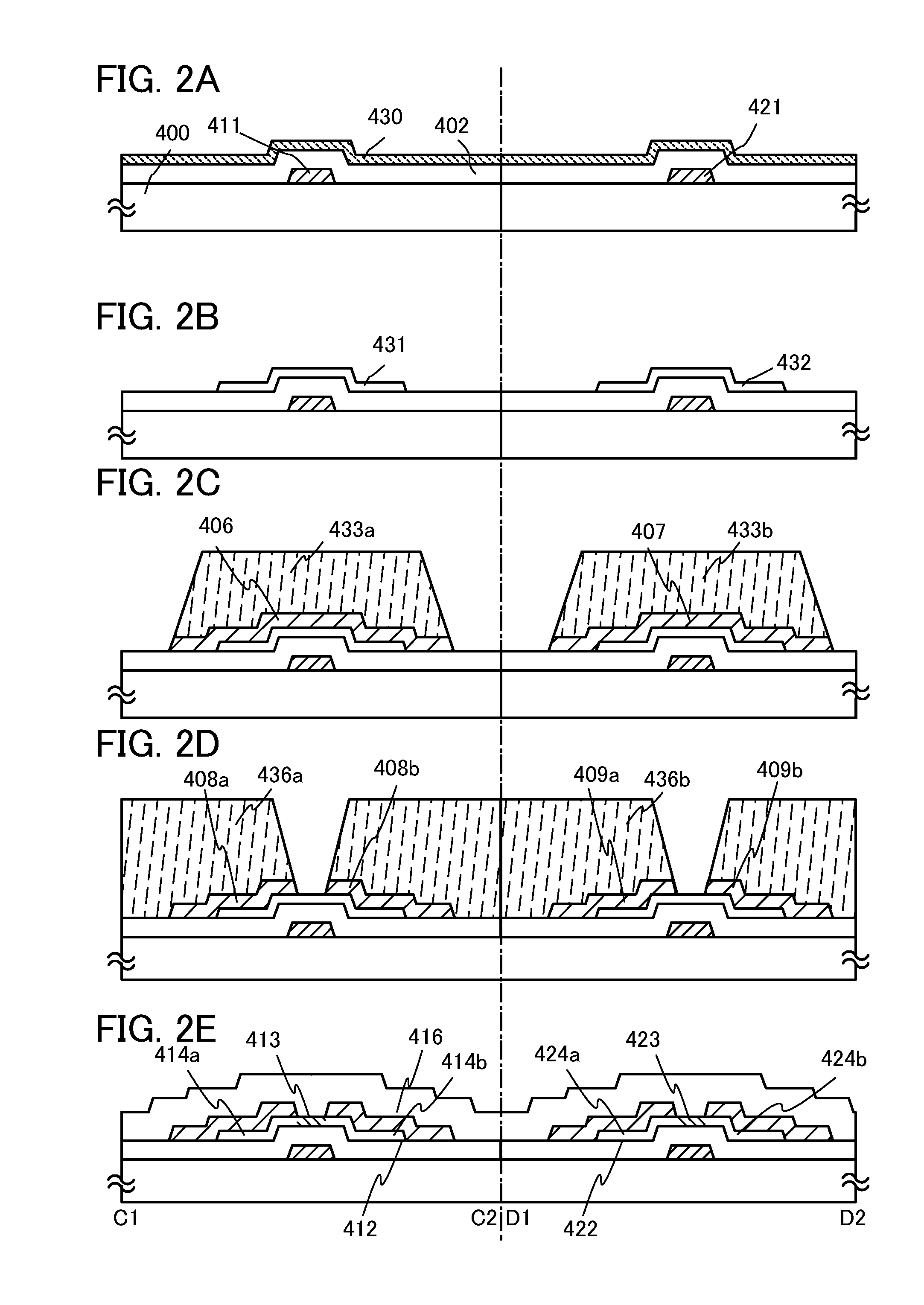
[0107]A semiconductor device and a method for manufacturing the semiconductor device will be described with reference to FIGS. 1A1, 1A2, 1B, and 1C, FIGS. 2A to 2E, and FIGS. 3A to 3D. FIGS. 1A1, 1A2, 1B, and 1C illustrate an example of a cross-sectional structure of two thin film transistors formed over one substrate. Thin film transistors 410 and 420 illustrated in FIGS. 1A1, 1A2, 1B, and 1C are thin film transistors having a bottom-gate structure.

[0108]FIG. 1A1 is a plan view of the thin film transistor 410 provided in a driver circuit. FIG. 1A2 is a plan view of the thin film transistor 420 provided in a pixel. FIG. 1B is a cross-sectional view illustrating a cross-sectional structure taken along line C1-C2 of FIG. 1A1 and a cross-sectional structure taken along line D1-D2 of FIG. 1A2. FIG. 1C is a cross-sectional view illustrating a cross-sectional structure taken along line C3-C4 of FIG. 1A1 and a cross-sectional structure taken along line D3-D4 of FIG. 1A2.

[0109]The thin film...

embodiment 2

[0188]In this embodiment, FIGS. 4A to 4C illustrates an example in which a first heat treatment is different from that of Embodiment 1. This embodiment is almost the same as Embodiment 1 except that a process is partly different from that of FIGS. 2A to 2E and FIGS. 3A to 3D. Therefore, the same portions are denoted by the same reference numerals and detailed description is omitted.

[0189]FIGS. 4A to 4C are cross-sectional views illustrating a manufacturing process of two thin film transistors.

[0190]First, according to the manufacturing process described in Embodiment 1, the gate electrode layers 411 and 421 are formed over the substrate 400 having an insulating surface.

[0191]The gate insulating layer 402 is formed over the gate electrode layers 411 and 421.

[0192]Next, the oxide semiconductor film 430 is formed to a thickness of greater than or equal to 2 nm and less than or equal to 200 nm over the gate insulating layer 402 (see FIG. 4A). Note that the process up to here is the same...

embodiment 3

[0206]A method for manufacturing a semiconductor device which is different from that in Embodiment 1 will be described with reference to FIGS. 5A to 5C. The same portions as Embodiment 1 or portions having functions similar to those of Embodiment 1 can be formed in a manner similar to that of Embodiment 1, and repetitive description thereof is omitted.

[0207]FIGS. 5A to 5C are cross-sectional views illustrating a manufacturing process of two thin film transistors.

[0208]First, in a similar manner to FIG. 2A of Embodiment 1, the gate electrode layers 411 and 421 are formed over the substrate 400 having an insulating surface, the gate insulating layer 402 is formed over the gate electrode layers 411 and 421, and the oxide semiconductor film 430 is formed over the gate insulating layer 402 (see FIG. 5A).

[0209]Next, a resist mask is formed over the oxide semiconductor film 430 by the second photolithography process. The oxide semiconductor film 430 is selectively etched using the resist m...


PUM


Abstract

The semiconductor device includes a driver circuit including a first thin film transistor and a pixel including a second thin film transistor over one substrate. The first thin film transistor includes a first gate electrode layer, a gate insulating layer, a first oxide semiconductor layer, a first oxide conductive layer, a second oxide conductive layer, an oxide insulating layer which is in contact with part of the first oxide semiconductor layer and which is in contact with peripheries and side surfaces of the first and second oxide conductive layers, a first source electrode layer, and a first drain electrode layer. The second thin film transistor includes a second gate electrode layer, a second oxide semiconductor layer, and a second source electrode layer and a second drain electrode layer each formed using a light-transmitting material.

Description

BACKGROUND OF THE INVENTION[0001]1. Field of the Invention[0002]The present invention relates to a semiconductor device including an oxide semiconductor and a manufacturing method thereof.[0003]Note that semiconductor devices in this specification mean all devices which can function by utilizing semiconductor characteristics, and electro-optical devices such as display devices, semiconductor circuits, and electronic devices are all semiconductor devices.[0004]2. Description of the Related Art[0005]In recent years, a technique by which a thin film transistor (TFT) is manufactured using a semiconductor thin film (having a thickness of approximately several nanometers to several hundred nanometers) formed over a substrate having an insulating surface has attracted attention. Thin film transistors have been applied to a wide range of electronic devices such as ICs or electro-optical devices and urgently developed particularly as switching elements in image display devices. Various metal...

Claims


Application Information

Patent Timeline
Patent Type & Authority Applications(United States)
IPC IPC(8): H01L29/786H01L21/44H05B44/00
CPCH01L27/1225H01L29/45H01L27/124H01L27/1255H01L27/1222H10K59/123H10K59/1213H01L27/1214H01L29/4908H01L29/7869H10K59/00
Inventor YAMAZAKI, SHUNPEISAKATA, JUNICHIROHOSOBA, MIYUKITAKAHASHI, TATSUYA
Owner SEMICON ENERGY LAB CO LTD
Why Eureka
Try Eureka