ESD protective device having low capacitance and stability and a preparing process thereof
a protective device and capacitance technology, applied in the direction of emergency protective arrangements for limiting excess voltage/current, semiconductor/solid-state device details, printing, etc., can solve the problems of esd protective characteristic change or not operate, difficult control process, and low capacitance stability characteristics
Inactive Publication Date: 2011-02-10
LATTRON
View PDF13 Cites 2 Cited by
- Summary
- Abstract
- Description
- Claims
- Application Information
AI Technical Summary
Benefits of technology
[0017]As above-illustrated, an ESD protective device capable of embodying a low capacitance and stability characteristics and a preparing process thereof according to the present invention make it possible to embody a characteristic easily and embody a characteristic of ESD parts stably since a voltage sensitive material utilizes property of particles itself but not property of grain boundary when preparing a voltage sensitive material being used in production of an ESD protective device different from ZnO based semiconductive ceramic materials utilizing property of grain boundary like prior art when preparing a voltage sensitive material, and provide an excellent property which does not distort a signal wave pattern when using as an ESD protective device of high signal line such as USB2.0, HDMI and the like since its permittivity is low so that it enables to embody low capacitance of 0.5 pF or lower.
Problems solved by technology
However, there has been a drawback that it is difficult to control the process during the calcination process.
Namely, there has been a drawback that an ESD protective characteristic is changed or do not operate in case where they face severe condition when thickness and components of a non linear resistance layer are changed by change of calcination process.
ZnO—based ceramic materials have a considerable defect in its permittivity so that it is beyond its capacity to employ it since an ESD protective device can not generally meet super low capacitance of 0.5 pF or lower when it is applied to high signal line.
However, its process becomes difficult since a dielectric layer is introduced.
Additionally, there is a drawback that there is a limitation in selection of a voltage sensitive material since a matching property (thermal expansion, chemical reaction) between a dielectric layer and a voltage sensitive material (320) should be considered.
Method used
View moreImage
Smart ImageViewing Examples

Examples
example 2
[0048]By following the same procedure as in the example 1, except that a green fluorescent substance for a conventional PDP is used as BaAl10O19:Mn and D50 is about 3.0 μm, an ESD protective device is produced.
example 3
[0049]By following the same procedure as in the example 1, except that a green fluorescent substance for a conventional PDP is used as Zn2SiO4:Mn and D50 is about 3.0 μm, an ESD protective device is produced.
example 4
[0050]By following the same procedure as in the example 1, except that a green fluorescent substance for a conventional inorganic EL(electro-luminescence) is used as ZnS:Cu and D50 is about 3.0 μm, an ESD protective device is produced.
Login to View More PUM
 Abstract
An ESD protective device having a low capacitance and stability characteristics constructed by installing a voltage sensitive material between electrodes. The voltage sensitive material comprises a fluorescent substance. The voltage sensitive material may be barium aluminate. The voltage sensitive material may be zinc silicate. The voltage sensitive material may be zinc sulfide. The voltage sensitive material is doped with a metal atom such as Mn, Cu and Eu. The device does not distort a signal wave pattern and have low capacitance of 0.5 pF or lower.
Description
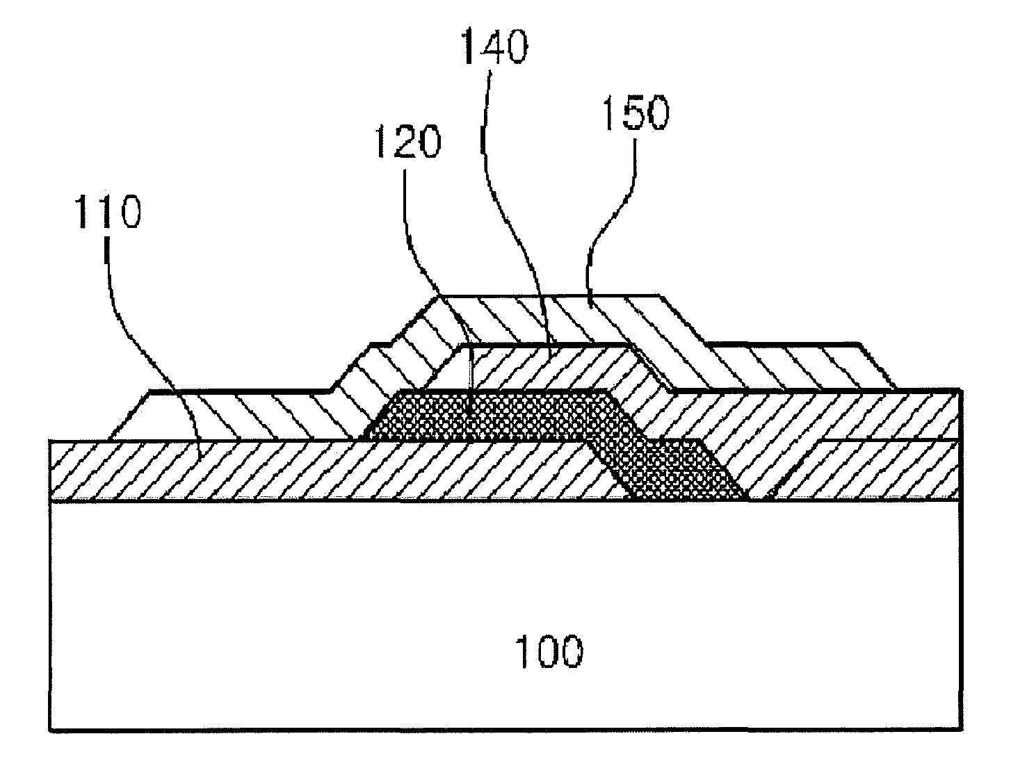
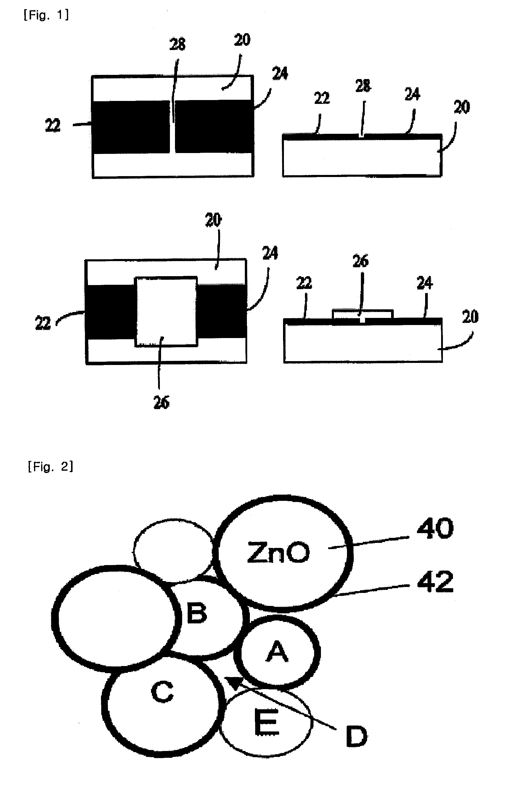
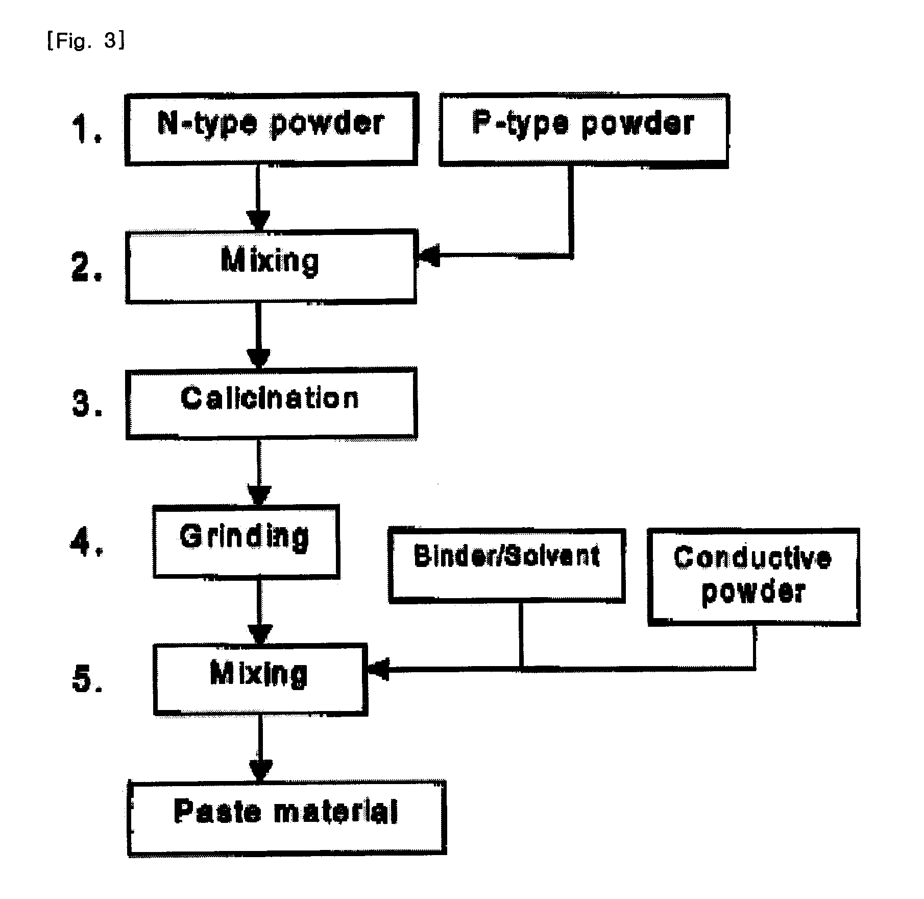
TECHNICAL FIELD[0001]The present invention relates to an ESD protective device having a low capacitance and stability and a preparing process thereof, more particularly to an ESD protective device having a low capacitance and stability and a simplified preparing process thereof, as compared to conventional ones, by using a voltage sensitive material which surmounts difficulty in forming the voltage sensitive material that has been used in production of an ESD protective device.BACKGROUND ART[0002]As shown at FIG. 1, there has been the structure in which an electrode is installed in the same plane or in a stacked form on a substrate and voltage protection material is installed therebetween in the prior art. Referring to FIG. 2, it has been used the voltage protection material which is produced by mixing at least two kinds of a semiconductive ceramic powder (for example, ZnO) and a conductive powder.[0003]As shown at FIG. 3, in the prior art, a voltage protection material results in f...
Claims
Login to View More Application Information
Patent Timeline
 IPC IPC(8): H02H9/04B41M1/12
CPCH01L23/60H01L27/0248H01L2924/0002H01L2924/00
Inventor LEE, CHUNG-KOOKLEE, WON-KYOUNG
Owner LATTRON