Data Path Read/Write Sequencing for Reduced Power Consumption

a data path and power consumption technology, applied in the field of solid-state memory, can solve the problems of chip area savings, power consumption of electronic circuitry in those devices and systems, and also of great concern, and achieve the effect of reducing power consumption

Active Publication Date: 2011-02-10
TEXAS INSTR INC
View PDF6 Cites 40 Cited by
  • Summary
  • Abstract
  • Description
  • Claims
  • Application Information

AI Technical Summary

Benefits of technology

[0009]Embodiments of this invention provide a memory and method of operating the same that r

Problems solved by technology

The power consumption of the electronic circuitry in those devices and systems is therefore of great concern, as battery life is often a significant factor in the buying decision as well as in the utility of the device or system.
However, as mentioned above, power consumption by the memory is also of great concern in these solid-

Method used


Image

  • Data Path Read/Write Sequencing for Reduced Power Consumption
  • Data Path Read/Write Sequencing for Reduced Power Consumption
  • Data Path Read/Write Sequencing for Reduced Power Consumption

Examples


Embodiment Construction

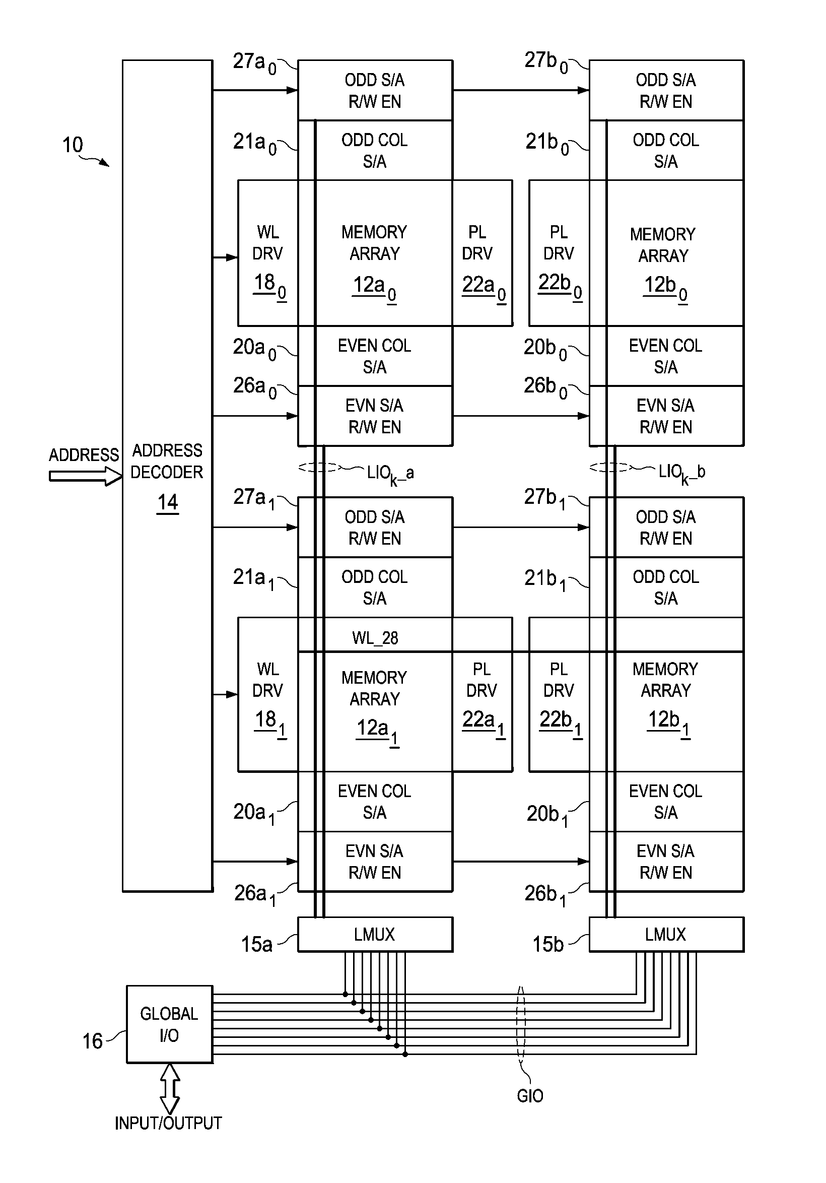
[0024]The present invention will be described in connection with its preferred embodiment, namely as implemented into a non-volatile solid-state memory of the ferroelectric random access memory (FeRAM) type. However, it is also contemplated that this invention can provide important advantages and benefits in other realizations, such as semiconductor memories of any type, including volatile static and dynamic RAM. In addition, while this description illustrates a stand-alone memory architecture, it is also contemplated that this invention may be implemented in embedded memories within large-scale integrated logic circuits, such as microprocessors or integrated circuits referred to as a “system-on-a-chip”. Accordingly, it is to be understood that the following description is provided by way of example only, and is not intended to limit the true scope of this invention as claimed.

[0025]FIG. 1 illustrates the architecture of memory 10 constructed according to embodiments of this inventi...


PUM


Abstract

A solid-state memory such as a ferroelectric random access memory (FeRAM) with multiplexed internal data bus and reduced power consumption on data transfer. The memory stores data in the form of multi-byte data words with error correction coding (ECC). In a page mode read/write operation, data states stored in memory cells of the selected row are sensed by sense amplifiers arranged in first and second banks, which are associated with first and second groups of columns. The first bank of sense amplifiers, associated with the first group of columns and containing the ECC value, are coupled to to the internal bus, followed by coupling the second bank of sense amplifiers associated with the second group of columns to the internal bus. The internal bus is then placed in tri-state, following which the internal data bus is driven with data to be written into the second group of columns in that same row, that data latched into the second bank of sense amplifiers. The internal bus is then driven with the data to be written to the first group of columns in the row, and latched into the first bank of sense amplifiers. To the extent that the data in the second group of columns does not change from the read to write operations, power consumption otherwise necessary for switching the internal bus is avoided.

Description

CROSS-REFERENCE TO RELATED APPLICATIONS[0001]This application claims priority, under 35 U.S.C. §119(e), of Provisional Application No. 61 / 158,182, filed Mar. 6, 2009, incorporated herein by this reference.STATEMENT REGARDING FEDERALLY SPONSORED RESEARCH OR DEVELOPMENT[0002]Not applicable.BACKGROUND OF THE INVENTION[0003]This invention is in the field of solid-state memory as realized in semiconductor integrated circuits. Embodiments of this invention are more specifically directed to the operation of data paths in such memories in read and write access operations.[0004]Many modern electronic devices and systems now include substantial computational capability for controlling and managing a wide range of functions and useful applications. Many of these electronic devices and systems are now portable or handheld devices. For example, many mobile devices with significant computational capability are now available in the market, including modern mobile telephone handsets such as those c...

Claims


Application Information

Patent Timeline
IPC IPC(8): G06F11/08
CPCG11C11/22G06F11/1048
Inventor MADAN, SUDHIR K.
Owner TEXAS INSTR INC
Why Eureka
Try Eureka