
Columnar Structure Film and Method of Forming Same, Piezoelectric Element, Liquid Ejection Apparatus and Piezoelectric Ultrasonic Oscillator
a technology of a structure film and a column structure, applied in the direction of device details, device material selection, piezoelectric/electrostrictive device details, etc., can solve the problems of poor practical applicability, low productivity, and extremely slow film formation rate, and achieve excellent driving durability, high voltage tolerance, and excellent voltage tolerance
- Summary
- Abstract
- Description
- Claims
- Application Information
AI Technical Summary
Benefits of technology
Problems solved by technology
Method used
Image

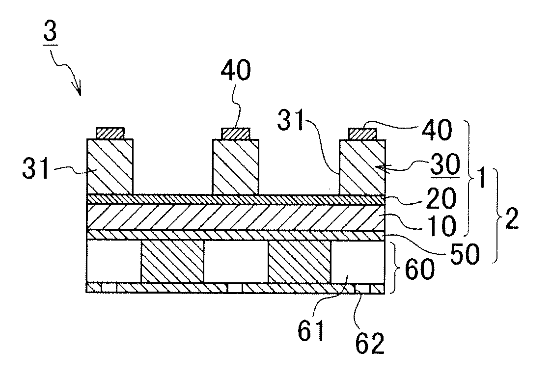
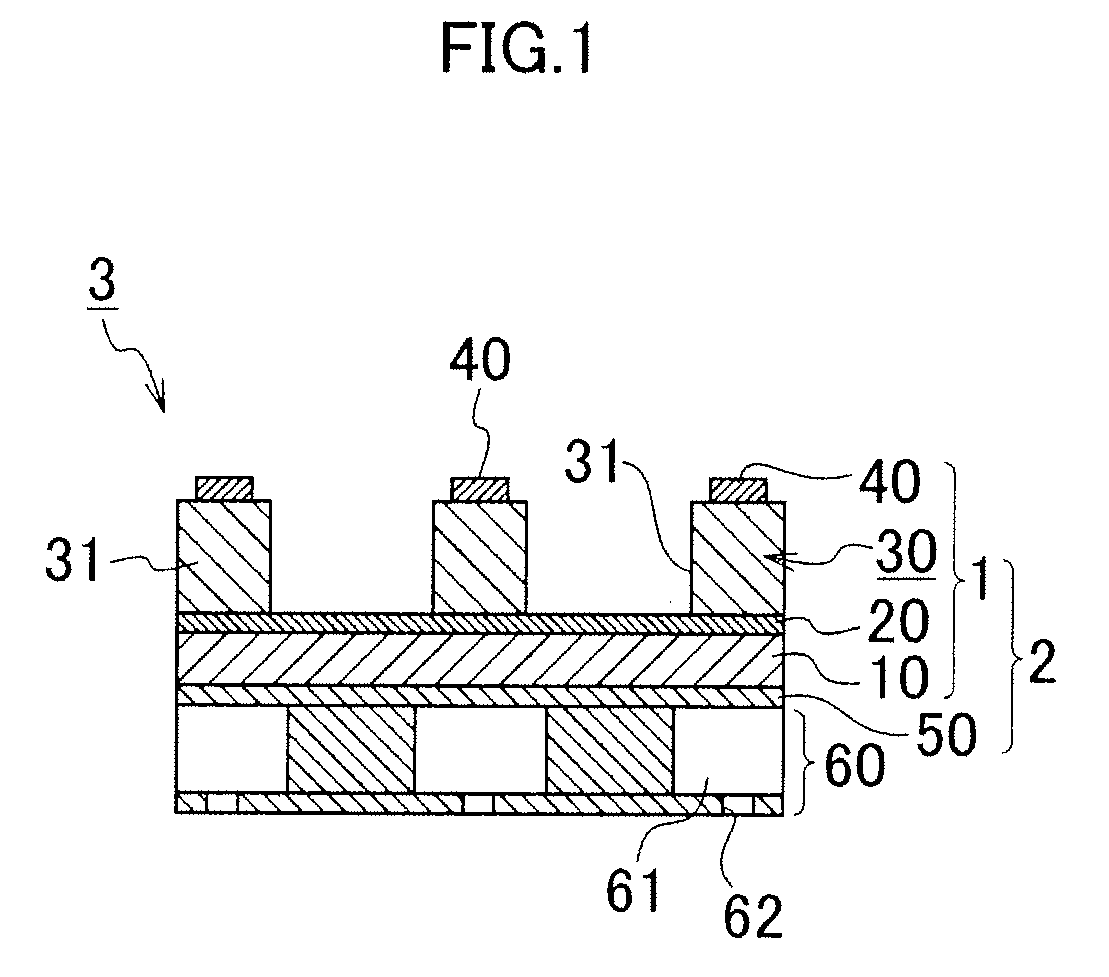
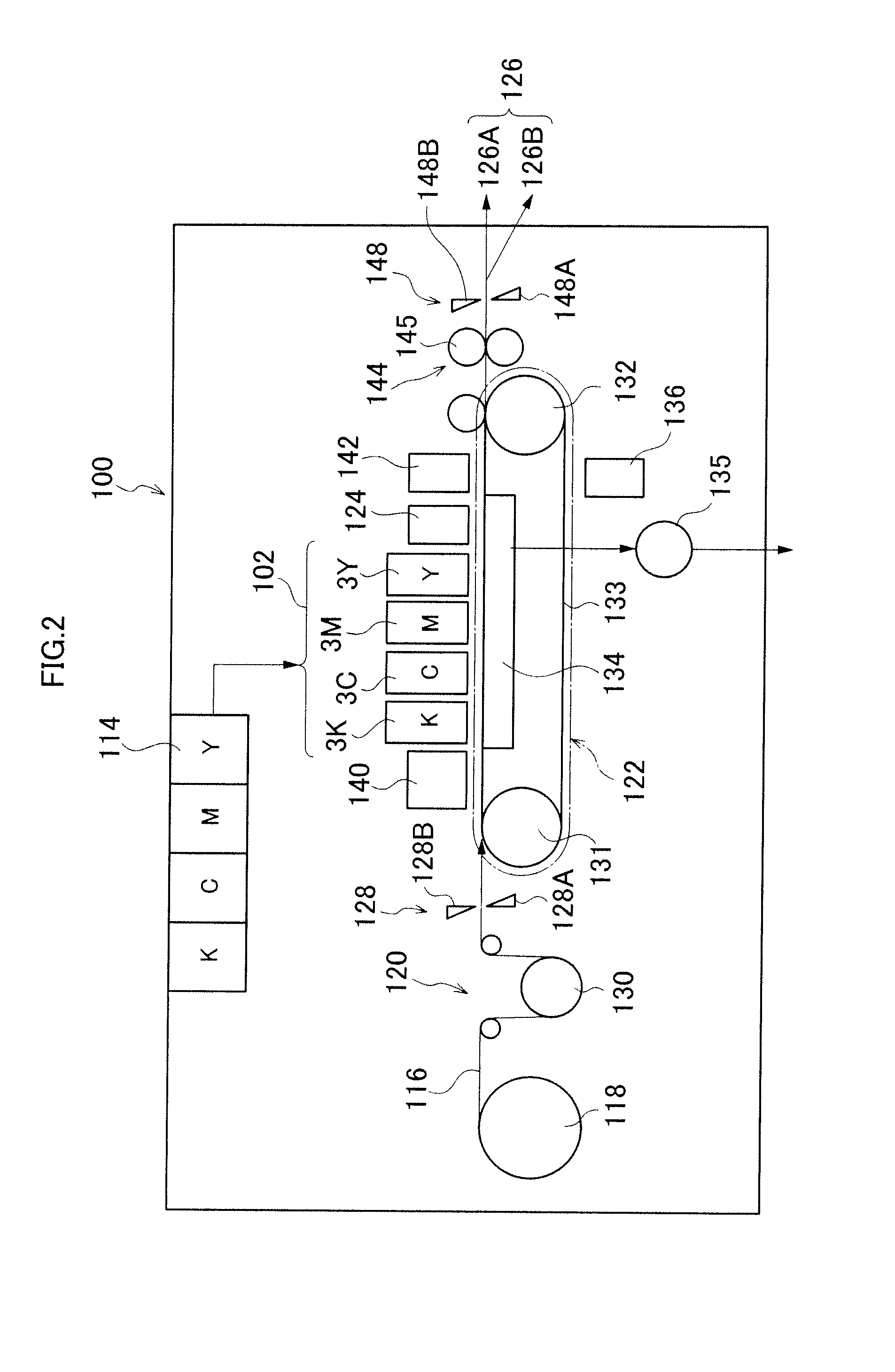
Examples
experimental example 1
[0101]A TiW film having a thickness of 50 nm and an Ir film having a thickness of 150 nm were successively deposited as a lower electrode on a silicon substrate by sputtering, at a substrate temperature of 350° C. A Nb-doped PZT piezoelectric film having a thickness of 3.9 μm was deposited over the lower electrode. The RF input power was altered during the course of deposition of the piezoelectric film. The film forming conditions were as described below.
[0102]Film forming apparatus: RF sputtering apparatus;
[0103]Target: 120 mm-diameter sintered body of Pb1.3(Zr0.46Ti0.42Nb0.12)O3;
[0104]Substrate temperature: 475° C.;
[0105]Target to substrate distance (T-S distance): 60 mm;
[0106]Film formation pressure: 0.3 Pa (2.3 mTorr);
[0107]Film formation gas: Ar / O2=97.5 / 2.5 (in mol ratio); and
[0108]Input power: 500 W for 40 minutes from start of film formation, and then 700 W for subsequent 30 minutes.
[0109]An electron backscatter diffraction (EBSD) measurement was carried out for the obtained ...
experimental example 2
[0114]A piezoelectric element for the purpose of comparison was obtained similarly to Experimental Example 1, apart from the fact that a piezoelectric film was formed under the same conditions from start to finish, rather than altering the film forming conditions of the piezoelectric film during the course of film formation. The film forming conditions of the piezoelectric film were as described below.
[0115]Film forming apparatus: same as Experimental Example 1;
[0116]Target: same as Experimental Example 1;
[0117]Substrate temperature: same as Experimental Example 1;
[0118]Target to substrate distance (T-S distance): same as Experimental Example 1;
[0119]Film formation pressure: same as Experimental Example 1;
[0120]Film formation gas: same as Experimental Example 1;
[0121]Input power: 500 W; and
[0122]Film formation time: 90 minutes.
[0123]An EBSD measurement was carried out for the obtained piezoelectric film. FIG. 6 shows a cross-sectional EBSD image of the piezoelectric film obtained in...
experimental example 3
[0127]Piezoelectric elements were obtained by forming a variety of piezoelectric films having different values for GSmax / GSmin, similarly to the Experimental Examples 1 and 2, by altering the film formation conditions variously. Table 2 shows film formation conditions.
TABLE 2Film formation conditionsFilmFilmVoltageT-SformationformationGSmax / GSmaxtolerancePowerPressureVDCdistancetimetemperatureGSmin(nm)(V)(W)(Pa)(V)(mm)(min)(° C.)1.571501504801.0−27080805201.602861254801.5−22080805201.751882055000.3−17060904751.802502254801.0−27090805202.402863505000.3−18560904753.00280450500 →0.3−170 →6040 →475600−190303.65300605500 →0.3−170 →6040 →475700−20030
[0128]In Table 2, the symbol “→” indicates that the film formation conditions were altered during the course of film formation similarly to the Experimental Example 1. In the table, “T-S distance” means the target to substrate distance, and “VDC” means the target self bias during the film formation.
[0129]Table 2 and FIG. 8 show the results of ...
PUM
| Property | Measurement | Unit |
|---|---|---|
| current | aaaaa | aaaaa |
| grain size | aaaaa | aaaaa |
| grain size | aaaaa | aaaaa |
Abstract
Description
Claims
Application Information