

Manufacturing method of microstructure
- Summary
- Abstract
- Description
- Claims
- Application Information
AI Technical Summary
Benefits of technology
Problems solved by technology
Method used
Image

Examples
embodiment 1
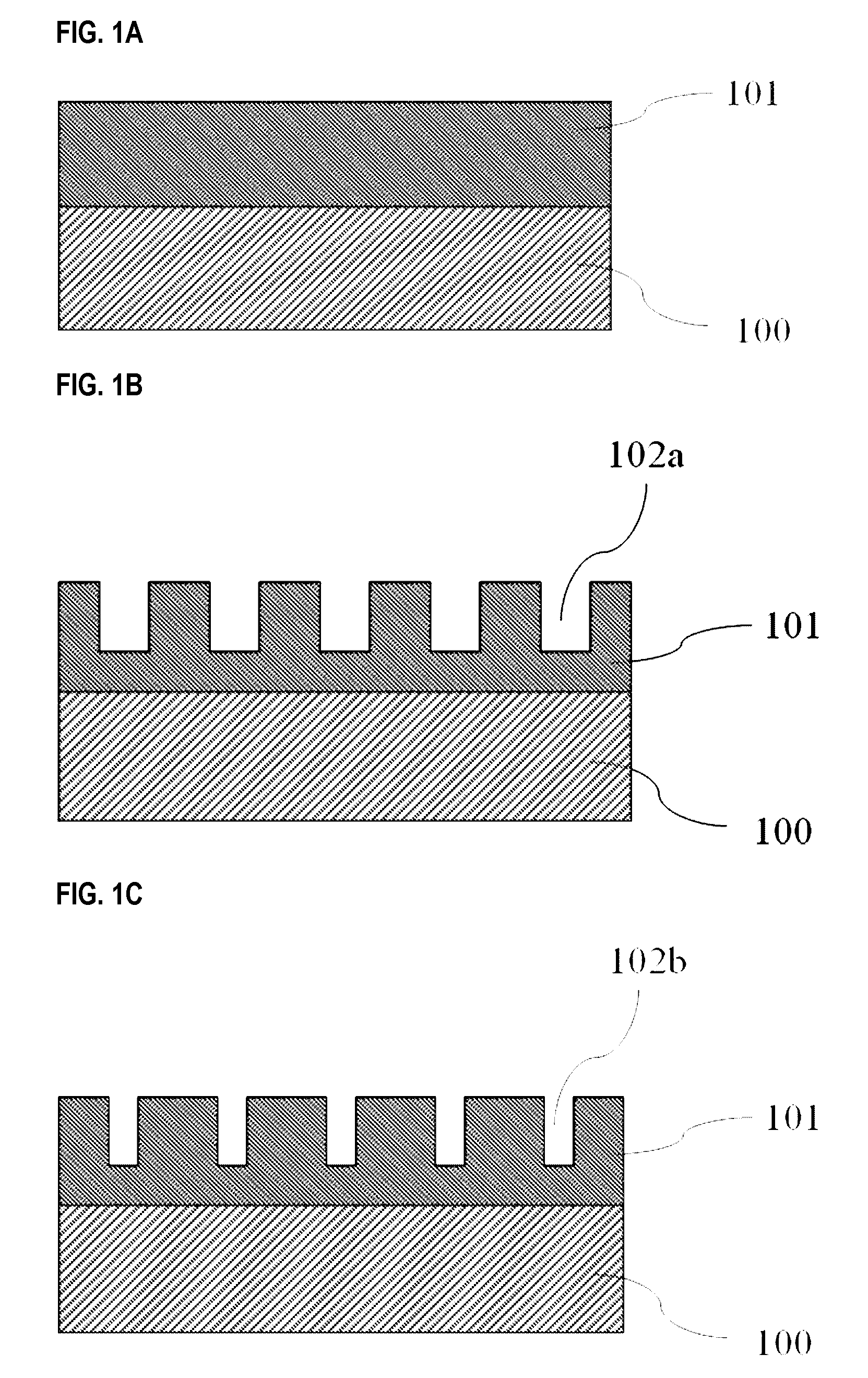
[0039]By using FIGS. 1A to 1C, a manufacturing method of a microstructure of a nitride semiconductor in embodiment 1 to which the present invention is applied will be described.
[0040](First Step)
[0041]First of all, in a first step, a first GaN semiconductor layer is formed on a substrate. In more concrete, as shown in FIG. 1A, a first GaN semiconductor layer 101 is stacked on a substrate 100 by an MOCVD method (Metalorganic Chemical Vapor Deposition), an HVPE method (Hydride Vapor Phase Epitaxy) and an MBE method (Molecular Beam Epitaxy). The substrate 100 used here may be of any material if only a GaN semiconductor can grow thereon, and for example, a substrate of sapphire, SiC, Si, GaAs, or GaN is used. Further, for the above described first GaN semiconductor 101, GaN, InN, AlN, AlGaN, InGaN, AlInN or AlGaInN is used.
[0042](Second Step)
[0043]Next, in a second step, a first hole 102a is formed in the above described first GaN semiconductor layer 101 by using etching. For this purpo...
embodiment 2
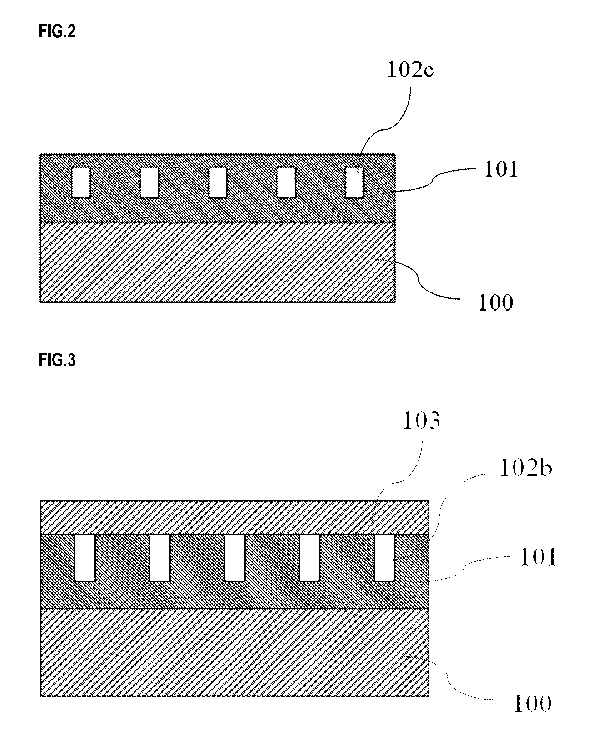
[0057]As embodiment 2, the mode of closing the second hole 102b by heat-treatment after the third step will be described by using FIG. 2. The present embodiment is the same as embodiment 1 up to the third step of making the first hole 102a narrow according to the heat-treatment of embodiment 1 to form the second hole 102b, and therefore, the description up to the third step will be described. In the present embodiment, as a fourth step, heat-treatment is performed in the gas atmosphere including nitrogen. In concrete, after the first hole 102a is made narrow and the second hole 102b is formed in the heat-treatment of the third step, heat-treatment is performed at a temperature higher than the temperature of the heat-treatment in the second step in the gas atmosphere including nitrogen. The gas atmosphere in the heat-treatment of the fourth step includes a nitrogen source in order to suppress desorption of nitrogen from the first GaN semiconductor as in the heat-treatment of the thir...
embodiment 3
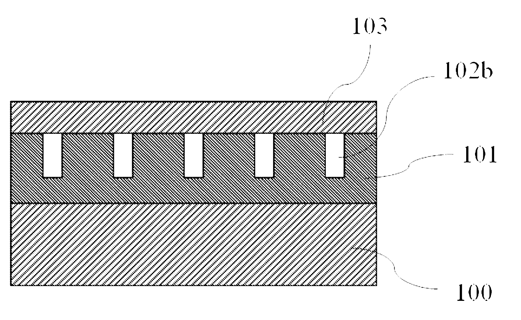
[0059]As embodiment 3, the mode of closing the second hole 102b with crystal growth after the third step will be described with use of FIG. 3. The present embodiment is the same as the embodiment 1 up to the third step of making the first hole 102a narrow to be formed into the second hole 102b of embodiment 1, and therefore, the description up to the third step will be omitted. In the present embodiment, after the first hole 102a is formed into the second hole 102b by the heat-treatment of the third step, the nitrogen raw material and the group III raw material are supplied as the fourth step. The second hole 102b has the structure narrow and depth with a high aspect ratio, and therefore, the group III raw material hardly reaches the bottom of the second hole 102b. As a result, the shape of the second hole 102b does not change significantly, and a second GaN semiconductor layer 103 can be formed on the first GaN semiconductor layer 101. The growth temperature of the second GaN semic...
PUM
 Abstract
Description
Claims
Application Information