Layered Chip For Use In Soldering

Active Publication Date: 2011-02-24
SEMIKRON ELECTRONICS GMBH & CO KG
View PDF5 Cites 5 Cited by
  • Summary
  • Abstract
  • Description
  • Claims
  • Application Information

AI Technical Summary

Benefits of technology

[0007]It is an object of the invention to eliminate the disadvantages according to the prior art. In particular, the intention is to produce a chip which can be produced as simply and cost-effectively as possibl

Problems solved by technology

In this case, it may happen that the layer assemblage produced from the metallic layers, in particular, is heated repeatedly to a temperature of from about 200 to about 250° C. When a soldering connection that has already been produced is reheated, it can happen that a new melt forms from the soldering layer and the so

Method used


Image

  • Layered Chip For Use In Soldering
  • Layered Chip For Use In Soldering

Examples


Embodiment Construction

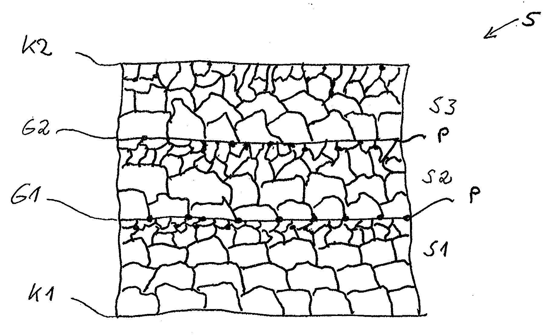
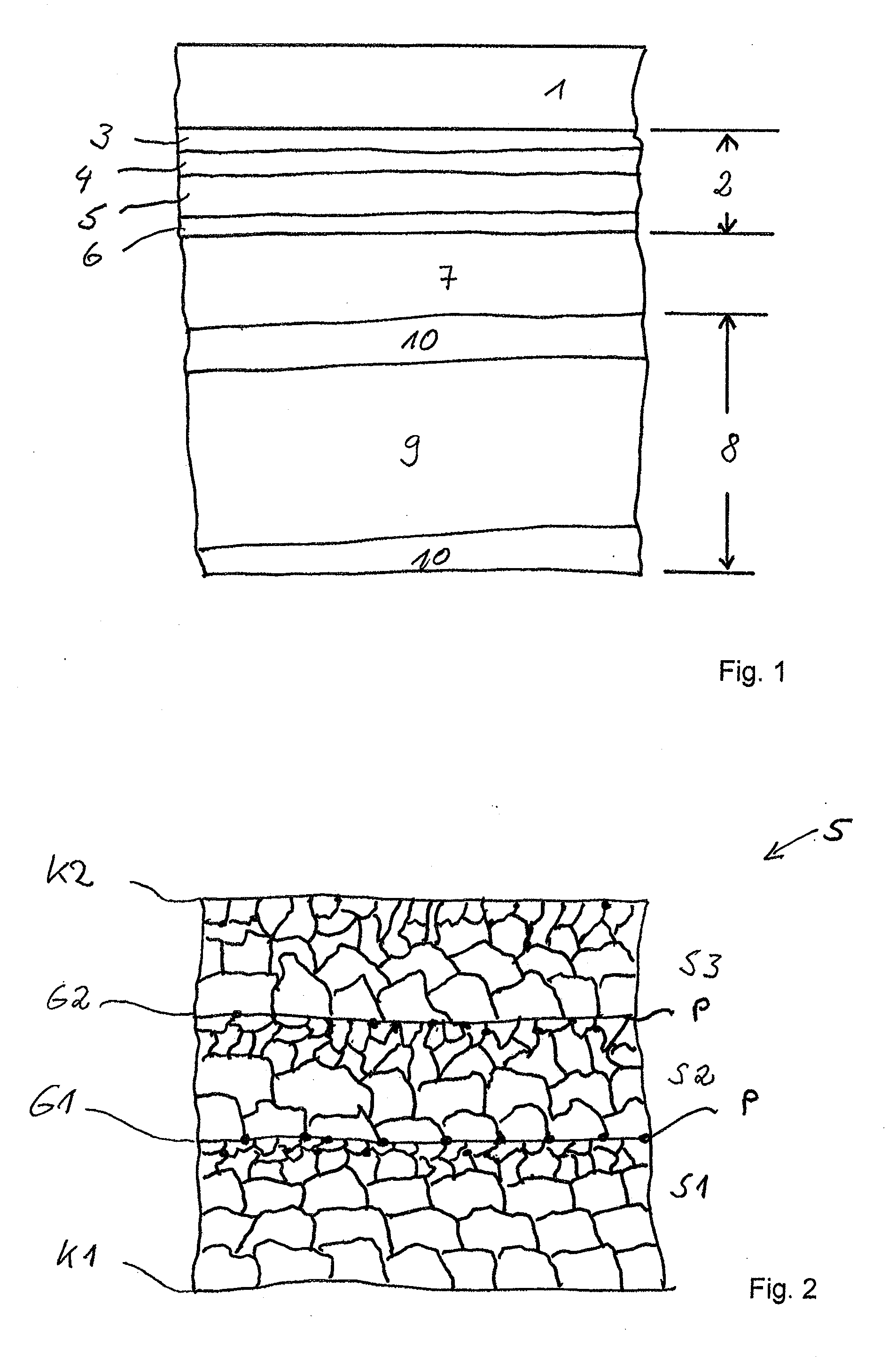
[0024]FIG. 1 shows a stylized cross-sectional view through a DCB substrate with a chip arranged thereon, wherein a soldering paste is provided between the chip and the DCB substrate. A fixed composite assembly of the chip with the DCB substrate can be produced from such an arrangement by supplying heat.

[0025]In FIG. 1, a chip body, designated generally by 1, is produced from Si, for example. A metallization is provided at one side of chip body 1, the metallization being formed from a layer assemblage, designated generally by 2. Layer assemblage 2 consists of a plurality of sequential metallic layers produced by means of a suitable physical coating method, such as PVD or sputtering. A base layer 3 is formed substantially from Al. A first intermediate layer 4 deposited thereon can substantially consist of a TiW alloy. A soldering layer 5 consisting of a plurality of layers (shown in more detail in FIG. 2) is deposited on first intermediate layer 4. Each of the layers can be produced f...


PUM


Abstract

A layer assemblage for a semiconductor chip having a chip body for producing a soldering connection for the chip. The assemblage is provided on a side of a chip body formed from a semiconducting material, wherein the layer assemblage is formed from a plurality of sequential metal layers which follow one above another and are produced by means of a physical coating method, and wherein a solderable soldering layer is provided between a noble metal layer situated at a surface of the layer assemblage and the chip body. In order to avoid an undesired penetration of a solder through the layer assemblage the soldering layer has at least one internal interface formed by an interruption of the coating method.

Description

BACKGROUND OF THE INVENTION[0001]1. Field of the Invention[0002]This invention is directed to a layered metal chip used to produce a soldering connection for a power semiconductor module.[0003]2. Description of the Related Art[0004]Known chips for producing power semiconductor modules are usually soldered onto a support, e.g. a Direct Copper Bonded (“DCB”) substrate or a metallic plate, for heat dissipation purposes. Reference is made to Lugscheider E. et al. “Spannungsreduktion in Chip-DCB-Verbunden mittels Ausnutzung der intrinsischen Spannungseigenschaften von PVD-Metallisierungsschichten” [“Stress reduction in chip-DCB composite assemblies by means of utilization of the intrinsic stress properties of PVD metallization layers”], Verbundwerkstoffe and Werkstoffverbunde [Composite materials and materials composites], M. Schimmerer (ed.), 2005. Soldering connections may furthermore be necessary for producing electrical connections.[0005]In order to produce the soldering connection, ...

Claims


Application Information

Patent Timeline
IPC IPC(8): H01L23/48H01L21/44
CPCH01L24/05H01L2924/00013H01L24/29H01L24/32H01L24/83H01L2224/04026H01L2224/32225H01L2224/32245H01L2224/83191H01L2224/83447H01L2224/83801H01L2924/01005H01L2924/01013H01L2924/01015H01L2924/01029H01L2924/01046H01L2924/01047H01L2924/0105H01L2924/01074H01L2924/01075H01L2924/01078H01L2924/01079H01L2924/01327H01L2924/014H01L2924/10329H01L2924/19043H01L2224/05H01L2224/29H01L2224/29298H01L2924/01006H01L2924/01023H01L2924/01024H01L2924/01033H01L2224/29101H01L24/27H01L2924/0132H01L2924/15724H01L2224/29111H01L2924/00H01L2924/01014H01L2924/01032H01L2924/01022H01L2924/01028H01L2924/01031H01L2924/00014H01L2224/29099H01L2224/29199H01L2224/29299H01L2224/2929H01L2924/15747H01L21/56H01L21/64H01L21/67
Inventor BERBERICH, SVEN
Owner SEMIKRON ELECTRONICS GMBH & CO KG
Why Eureka
Try Eureka