Method of welding printed circuit board containing mixed lead components and leadless components

A printed circuit board and welding method technology, which is applied in the direction of assembling printed circuits with electrical components, welding media, welding equipment, etc. The effect of avoiding the decrease of solder joint reliability, avoiding the deformation of printed circuit boards, and reducing the difficulty of material control

Active Publication Date: 2009-10-07
BEIJING RES INST OF TELEMETRY +1
View PDF0 Cites 15 Cited by
  • Summary
  • Abstract
  • Description
  • Claims
  • Application Information

AI Technical Summary

Problems solved by technology

In this case, there are problems that are difficult to solve no matter whether the lead process, lead-free process or lead / lead-free soldering process is used
[0003] If there is no distinction between leaded components and lead-free components, and they are soldered according to the traditional lead-based process, then most lead-free devices will not completely melt the lead-free solder end plating or solder balls due to the low soldering temperature, making the components The interface on one side cannot generate intermetallic compounds that meet the requirements, resulting in virtual soldering
Therefore, if lead-free devices cannot be effectively identified, serious quality problems will occur when soldering mixed printed board assemblies using a purely lead-based process
[0004] If the lead-free process is adopted, both the solder and the solder end can be fully melted, but for the soldering of mixed printed board assemblies, this process also has many difficult problems: first, the temperature resistance of leaded devices will be reduced Under the severe test, some leaded devices will degrade or even fail due to the high lead-free soldering temperature; secondly, use lead-free solder (the mainstream is SnAg3.5Cu0.5) to solder the leaded components whose pin plating is Sn-Pb alloy At the same time, Pb segregation is easily formed at the interface between the solder and the pad, that is, the low melting point layer of Sn-Ag-Pb at 174 ° C is formed, and the thermal stress during the secondary soldering will cause the solder joint to peel off from the pad, which is the so-called Lift-off (solder joint peeling) phenomenon; third, when using lead-free solder to solder leaded BGA, the leaded solder on the solder ball melts first, covering the pad and component soldering end, and the flux cannot be discharged, causing pores. Affects solder joint reliability
This process scheme is feasible in principle, and it avoids the above-mentioned problems caused by the mismatch between the solder and the device, but there are huge difficulties in its implementation: First, after the lead-free components are soldered, the entire board cannot be coated Solder paste with lead can only be coated by hand and partial stencil, which is unacceptable in terms of solder paste coating effect and production efficiency; secondly, the control of materials on the production site is extremely difficult, and manual distinction is required And control lead and lead-free solder paste and components, when mass producing high-density assemblies, it is almost impossible to face thousands of components in different states without errors
It can be seen that the separate soldering of leaded / lead-free components can only be applied to products with small production batches, low assembly density, and manual soldering
However, for the production of high-density printed board assemblies containing a large number of multi-pin, narrow-pitch devices, this process scheme is basically infeasible
[0006] To sum up, the existing conventional process methods cannot effectively solve the problem of mixed packaging, and the mixed packaging of leaded components and lead-free components has brought huge challenges to electronic assembly technology

Method used


Image

  • Method of welding printed circuit board containing mixed lead components and leadless components
  • Method of welding printed circuit board containing mixed lead components and leadless components
  • Method of welding printed circuit board containing mixed lead components and leadless components

Examples


Embodiment 1

[0054] 1. Basic components:

[0055] 1) Printed circuit board

[0056] The main factors affecting the quality of solder joints are: welding process parameters, printed board materials and coating materials, pin coatings of lead-free components, welding times, environmental tests, etc. In order to compare and analyze the influence trend of various influencing factors on soldering quality, in this embodiment, two types of printed boards are designed to install various types of lead-free devices and chip components, wherein: the board is epoxy glass laminated board (FR4 ), the surface coating is a lead-tin alloy printed board, numbered board A1-01; the board is epoxy glass laminated board (FR4), and the surface coating is electroless nickel-plated immersion gold 1 printed board, numbered Plate A2-01. In order to avoid the influence of other factors on the test results, the design of the test circuit board is simplified as far as possible, and the device density is low. The tes...

Embodiment 2

[0100] 1. Basic components

[0101] 1) Printed circuit board

[0102] Select a printed board with epoxy glass laminate (FR4) and lead-tin alloy as the surface coating, numbered board A1-02; the plate is epoxy glass laminate (FR4), and the surface coating is electroless nickel plating 1 printed board of gold, numbered board A2-02, the rest are the same as "embodiment 1".

[0103] 2) Leaded components and lead-free components

[0104] Same as Example 1

[0105] 3) Solder and flux

[0106] Same as Example 1

[0107] 4) Instruments and equipment

[0108] Same as Example 1

[0109] 2. Test steps

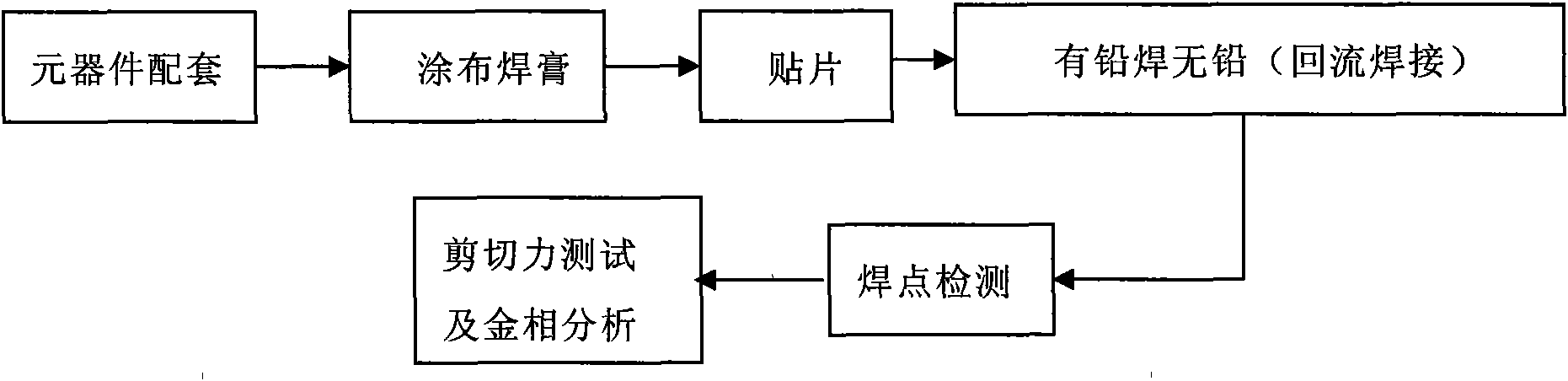
[0110] 1) Inspection and matching of components

[0111] Same as Example 1

[0112] 2) Coating solder paste

[0113] Same as Example 1

[0114] 3) patch

[0115] Same as Example 1

[0116] 4) Reflow soldering

[0117] Put the printed circuit board into the reflow furnace with 9 temperature zones for soldering, and control the peak temperature to 215°C, such as Figure 5 Sho...

Embodiment 3

[0123] 1. Basic components

[0124] 1) Printed circuit board

[0125] Select a printed board with epoxy glass laminate (FR4) and lead-tin alloy as the surface coating, numbered board A1-03; the plate is epoxy glass laminate (FR4), and the surface coating is electroless nickel plating 1 printed board of gold, numbered board A2-03, the rest are the same as "embodiment 1".

[0126] 2) Leaded components and lead-free components

[0127] Same as Example 1

[0128] 3) Solder and flux

[0129] Same as Example 1

[0130] 4) Instruments and equipment

[0131] Same as Example 1

[0132] 2. Test steps

[0133] 1) Inspection and matching of components

[0134] Same as Example 1

[0135] 2) Coating solder paste

[0136] Same as Example 1

[0137] 3) patch

[0138] Same as Example 1

[0139] 4) Reflow soldering

[0140] Put the printed circuit board into the reflow furnace with 9 temperature zones for soldering, and control the peak temperature at 225°C, such as Figure 6 Sho...


PUM

PropertyMeasurementUnit
melting pointaaaaaaaaaa

Abstract

The present invention relates to a method of welding printed circuit board containing mixed lead components and leadless components, using lead solder and controlling welding temperature curve to improve welding peak temperature and prolong solder liquid phase time properly on the base of conventional lead welding technics to implement reliable welding of leadless components. Applying the invention provided technical scheme can implement solder paste coating, patching and welding in one time of most lead components and leadless components, of which the production efficiency is far higher than separate welding technics of lead components and leadless components. The invention provided method improves production efficiency and reduces materials control difficulty of production field while shorts production period of mixed products and reduces production cost.

Description

technical field [0001] The invention relates to the technical field of electronic assembly, in particular to a welding method for a mixed printed circuit board assembly with lead components and lead-free components. Background technique [0002] With the advancement of lead-free electronic products, most of the components are lead-free components or lead and lead-free coexist. In foreign countries, in order to ensure the long-term reliability of aerospace electronics, medical electronics and other products, the above products are not subject to the RoHS and WEEE directives. However, due to the status quo of my country's military industry, that is, the main functional electronic components used still rely on foreign imports and are subject to foreign embargoes, it is impossible to obtain leaded electronic components above military grades, and only industrial-grade lead-free electronic components can be used. . As a result, the domestic military electronics industry must face...

Claims


Application Information

Patent Timeline
Patent Type & Authority Applications(China)
IPC IPC(8): H05K3/34B23K1/20B23K1/008B23K35/24B23K35/362
Inventor 何伟毛春霞刘芳齐凤海赵志勇田军霞
Owner BEIJING RES INST OF TELEMETRY
Why Eureka
Try Eureka