

Photodetector and display device
- Summary
- Abstract
- Description
- Claims
- Application Information
AI Technical Summary
Benefits of technology
Problems solved by technology
Method used
Image

Examples
embodiment 1
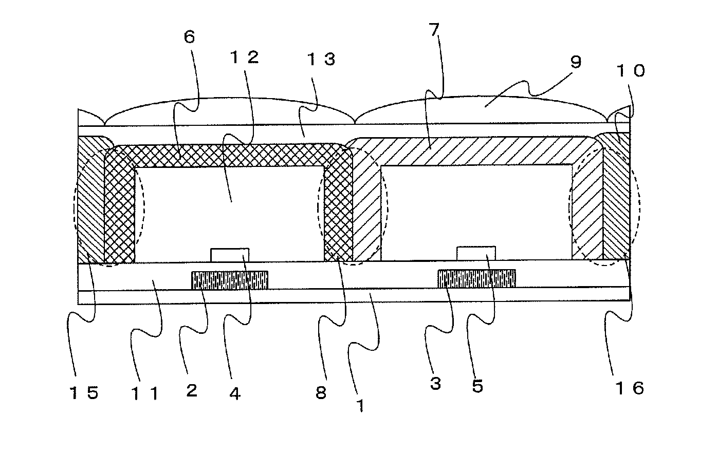
[0028]A photodetector which is one mode of the present invention will be described (FIG. 1A). FIG. 1A is a cross-sectional view of the photodetector.
[0029]The photodetector which is one mode of the present invention includes a first light-blocking layer 2 and a second light-blocking layer 3 over a substrate 1 having a light-transmitting property, a first photodiode 4 over the first light-blocking layer 2, a second photodiode 5 over the second light-blocking layer 3, a first color filter 6 covering the first photodiode 4, and a second color filter 7 covering the second photodiode 5. The photodetector includes a third light-blocking layer 8 formed with the first color filter 6 and the second color filter 7 between the first photodiode 4 and the second photodiode 5. The photodetector also includes microlenses 9 over the first color filter 6 and the second color filter 7 with a third light-transmitting insulating film 13 interposed therebetween.
[0030]In order to collect light to the pho...
example 1
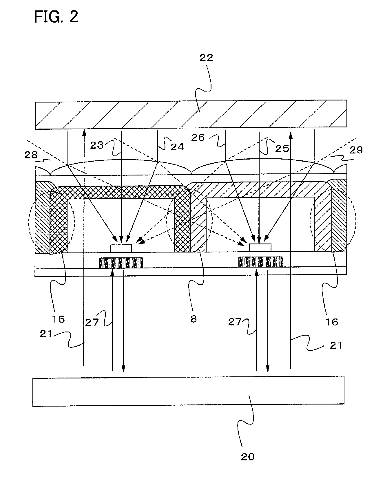
[0071]A liquid crystal display device which is one mode of the present invention will be described (FIGS. 6 and 7). FIG. 6 is a cross-sectional view of the liquid crystal display device, and FIG. 7 is a top view of a pixel portion of the liquid crystal display device.
[0072]The display device which is one mode of the present invention has a photodetection portion A-A′ and a display portion B-B′.
[0073]A top schematic view of the pixel portion of the display device is illustrated in FIG. 7. The photodetection portion A-A′ of FIG. 6 corresponds to an A-A′ portion of FIG. 7, and the display portion B-B′ of FIG. 6 corresponds to a B-B′ portion of FIG. 7.
[0074]Note that a photodetection method in the liquid crystal display device of this example is basically similar to Embodiment 1. Light emitted from a backlight below the substrate 1 having a light-transmitting property is transmitted through the substrate 1 and the first color filter 6 or the second color filter 7 and reflected off a por...
example 2
[0117]An electroluminescent display device (hereinafter referred to as an “EL display device”) which is one mode of the present invention will be described below.
[0118]FIG. 8 illustrates an example of a cross-sectional view of an EL display element with an EL element (for example, an organic EL element, an inorganic EL element, or an EL element including an organic substance and an inorganic substance) used as a light-emitting element. The display device of Example 1 and the light-emitting device of this example are different in that the display device of Example 1 has the liquid crystal element, the first light-blocking layer 2, the second light-blocking layer 3, and the light-blocking layer 58, while the light-emitting device of this example has the EL element and does not have the first light-blocking layer 2, the second light-blocking layer 3, and the light-blocking layer 58. The photodetection method of the display device of Example 1 and that of the light-emitting device of Ex...
PUM
 Abstract
Description
Claims
Application Information