Method for manufacturing a multi-layer stack structure with improved wvtr barrier property

a technology of multi-layer stack structure and barrier property, which is applied in the direction of manufacturing tools, surface layering apparatus, thermoelectric devices, etc., can solve the problems of deformation of liquid crystal in liquid crystal cells, poor gas barrier properties, and display failure of degraded parts, etc., and achieve excellent barrier properties to water vapour, efficient and cheap process, and good gas barrier properties

Inactive Publication Date: 2011-03-03
FUJIFILM MFG EURO
View PDF32 Cites 18 Cited by
  • Summary
  • Abstract
  • Description
  • Claims
  • Application Information

AI Technical Summary

Benefits of technology

[0016]The present invention provides an effective, efficient and cheap process for manufacturing of flexible multi-layer material with excellent barrier property to water vapour. Furthermore, this invention provides flexible multi-layer material with an excellent barrier property to water vapour.
[0018]By simultaneously treating two substrates in the single treatment space and subsequent laminating of the two substrates, a very efficient production process is obtained resulting in a multi-layer stack structure having very good water vapour transmission rate characteristics. Furthermore, the chance of impurities or other contaminations reaching the substrates before laminating is reduced. Also, a more uniform treatment of the substrates is achieved when using a single treatment space. It has been found that the present method may be applied to improve certain characteristics when applying layers of material to the two substrates (films or foils) and after laminating these into one multi-layer stack structure (again a roll of film or foil). Using the present invention embodiments allows to provide for deposition rates of more than 1 nm / s, e.g. 5 nm / s or even 10 nm / s.
[0020]The substrates are provided as sheets to obtain the multi-layer stack structure in a continuous process. For example, the substrates may be provided from two rolls with a predetermined width, and the laminated structure may be spooled on a receiving roll. This two roll to one roll process is very efficient for continuous manufacturing of the multi-layer stack structure, by adhering the two treated substrates with the treated surfaces facing each other by lamination into one roll using an adhesive.
[0023]In a further embodiment, the step of treating the facing surfaces is executed with a duty cycle above 10%, preferably above 60%. This effectively reduces the formation of dust when depositing the inorganic layer on the substrates.
[0024]An atmospheric pressure glow discharge is generated in a further embodiment by applying electrical power from a power supply to the at least two electrodes in the treatment space during an on-time (ton), the treatment space being filled with a gas composition, including a precursor of the chemical compound or element to be deposited, wherein the gas composition comprises an amount of nitrogen between 1 and 99.99% and an amount of oxygen between 0.01 and 25%. Again, this reduces the chance of formation of dust in the deposition step and an improvement of the quality of the deposited layer.

Problems solved by technology

However, the film substrate of transparent plastics or the like is problematic in that its gas-barrier property is not good as compared with that of glass.
When a substrate having a poor gas-barrier property is used, water vapor and air may penetrate through it; and, for example, when it is used in liquid-crystal display devices, the liquid crystal in the liquid-crystal cell may be degraded and the degraded part may be a display failure, thereby worsening the display quality of the devices.
However, with recent development of large-panel liquid-crystal display devices and high-definition display devices, the film substrate is being required to have a water-vapor barrier level of about 0.1 g / m2.day.
However, when a film substrate is used, the substrate temperature is limited in layer formation thereon, and therefore a barrier layer having a sufficiently dense and tight structure could not be formed, and a film having a satisfactory barrier property capable of satisfying the requirements could not as yet be formed.
However, the constitution could not satisfy both a sufficient gas-barrier level and a bending resistance which the film substrate must have in its use, and further technical improvement on it is desired.
However, the adhesiveness between the organic layer and the inorganic layer is not always satisfactory, and a multi-layered structure of at least 6 layers is needed for providing a high-reliability barrier film for organic EL devices.

Method used


Image

  • Method for manufacturing a multi-layer stack structure with improved wvtr barrier  property
  • Method for manufacturing a multi-layer stack structure with improved wvtr barrier  property
  • Method for manufacturing a multi-layer stack structure with improved wvtr barrier  property

Examples


examples

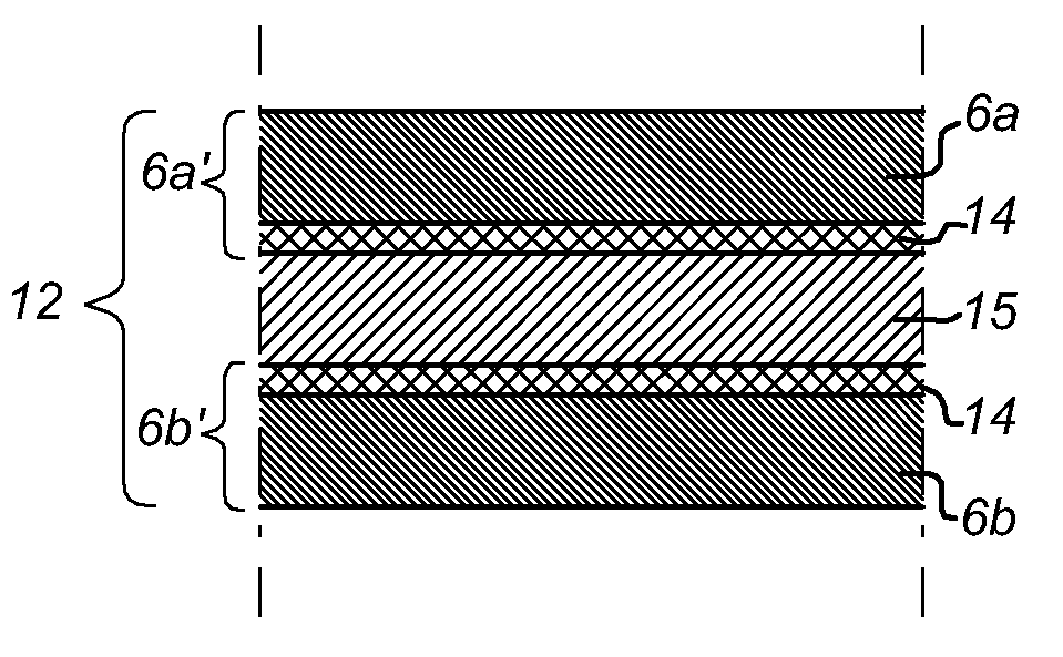
[0070]As a substrate material 6a, 6b optical grade PEN was used having a thickness of 90 micron. WVTR of the PEN substrate without coating was quantified by Mocon Aquatran and is typically 0.27+ / −0.03 g / m2.day .

example 1

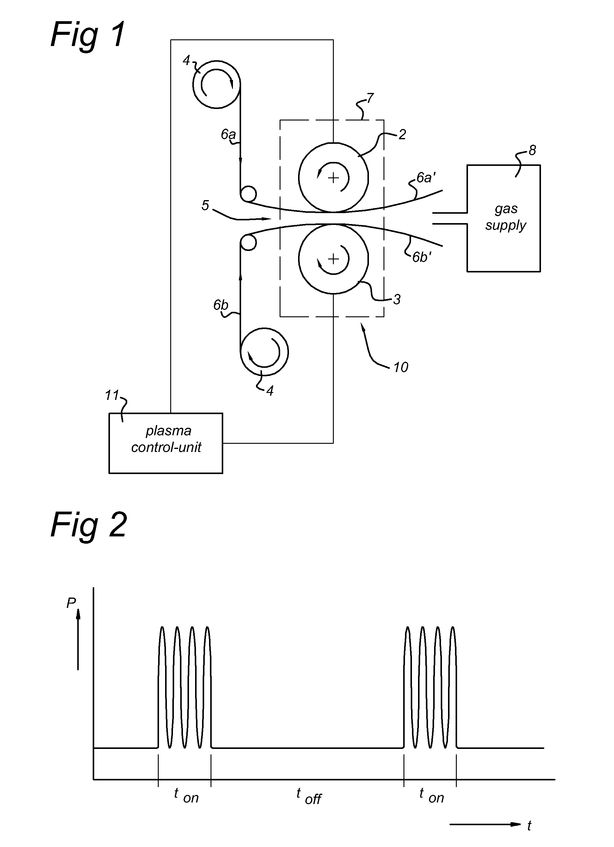
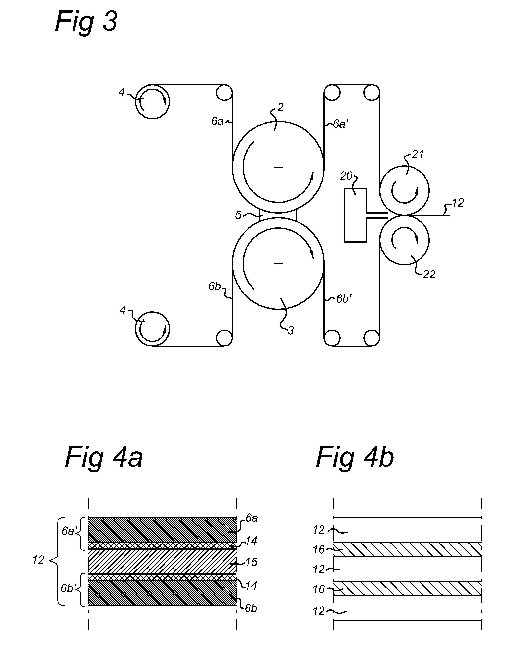
[0075]Two barrier films 14 of 50 nm thick are deposited synchronously using the electrode set-up as shown in FIG. 1 using an atmospheric pressure plasma device 10. On both sides of the substrates 6a, 6b facing the plasma discharge a SiOx layer 14 is deposited. Directly, after depositing the inorganic layer 14 the two substrates 6a′, 6b′ are brought together and laminated with the same hydrophobic acrylate as above with a thickness of 10 micron followed by UV-curing. Under the same conditions more barrier samples are produced and part of this material is prepared for permeability characterization by Mocon.

[0076]The WVTR of the individual layers 6a′, 6b′ is typically 0.03 g / m2.day, whereas the permeability of the laminate structure 12 is typically less than 1*10−3 g / m2.day.

example 2

[0077]Two barrier films 14 of 100 nm thick are deposited in one time using the electrode set-up as shown in FIG. 1. On both sides of the substrates 6a, 6b facing the plasma discharge a SiOx layer 14 is deposited. Directly, after depositing the inorganic layer 14 the two substrates 6a′, 6b′ are brought together and laminated using the same thickness and same acrylate layer 15.

[0078]Under same conditions more barrier samples are produced, part of this material is sampled for permeability characterization by Mocon.

[0079]WVTR of the individual layers 6a′, 6b′ is typically 0.03 g / m2.day, whereas the permeability of the laminate structure 12 is below the detection limit of the Mocon Aquatran.

[0080]Subsequently, the permeability is characterized by the calcium corrosion test. This method allows characterization of the average WVTR as low as 10−5 to 10−6 g / m2.day at 40° C. / 90% RH. The WVTR for the multi-layer stack structure 12 was found to be typically in the order of 10−4 g / m2.day.

[0081]M...


PUM

PropertyMeasurementUnit
deposition ratesaaaaaaaaaa

Abstract

A method and apparatus for manufacturing a multi-layer stack structure (12), the structure (12) comprising in order: a substrate (6a) a barrier layer (14) an adhesive layer (15) a barrier layer (14) a substrate (6b). The method comprises: a) providing two substrates (6a, 6b) in a single treatment space (5), the treatment space (5) comprising at least two electrodes (2, 3) for generating an atmospheric pressure glow discharge plasma in the treatment space (5); b) treating the facing surfaces of the two substrates (6a, 6b) simultaneously in the single treatment space (5); c) laminating the two treated substrates (6a, 6b) with an adhesive layer (15) in between the facing surfaces to obtain the multi-layer stack structure (12).

Description

TECHNICAL FIELD[0001]The present invention relates to a method for manufacturing a multi-layer stack structure, the structure comprising in order:a substrate—a barrier layer—an adhesive layer—a barrier layer—a substrate.[0002]Furthermore, this invention relates to a device, e.g. an OLED device comprising such a multi-layer stack structure.[0003]In an even further aspect, the present invention relates to an apparatus for producing a multi-layer stack structure, the apparatus comprising a treatment space with at least two electrodes connected to a plasma control unit for generating an atmospheric pressure glow discharge plasma in the treatment space, and a gas supply device in communication with the treatment space for providing compounds (gases and precursors) in the treatment space.BACKGROUND ART[0004]International patent application WO99 / 04411 discloses plasma treatment systems and treatment methods, in which a substrate web is treated using cylindrical cavity electrodes. Direct pl...

Claims


Application Information

Patent Timeline
Patent Type & Authority Applications(United States)
IPC IPC(8): H01L51/50H01L51/56H01L21/64C23C16/00B32B38/00
CPCH01L51/5237H05H1/24H01L2251/5338H05H1/48H05H2240/10H05H1/473H10K2102/311H10K59/8731H10K50/844
Inventor DE VRIES, HINDRIK WILLEMVAN DE SANDEN, MAURITIUS CORNELIUS MARIA
Owner FUJIFILM MFG EURO
Why Eureka
Try Eureka