Thin film photoelectric conversion device and method for manufacturing the same

Active Publication Date: 2011-03-17
KANEKA CORP
View PDF6 Cites 7 Cited by
  • Summary
  • Abstract
  • Description
  • Claims
  • Application Information

AI Technical Summary

Benefits of technology

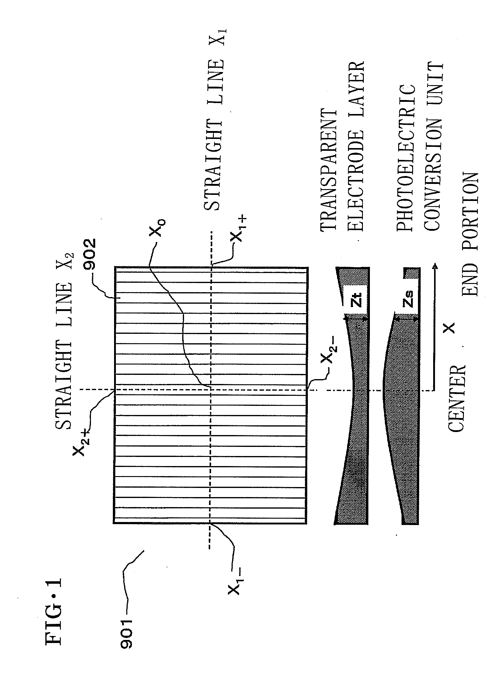
[0014]As described in Patent Document 1, in formation of the photoelectric conversion unit constituting the integrated-type thin film photoelectric conversion device, a plasma enhanced CVD method capable of making its area large and its cost low is often used. A film thickness of the photoelectric conversion layer formed by this method often has a distribution based upon film-forming positions inside a plasma enhanced CVD device. For example, when a reaction gas is supplied inside the plasma enhanced CVD device from the central portion to the substrate, a film thickness of a photoelectric conversion layer grown in a position close to a reaction gas supply portion (central portion of the substrate) tends to be larger, whereas a film thickness of a photoelectric conversion layer grown in a position far from the reaction gas supply portion (peripheral portion of the substrate) tends to be smaller.
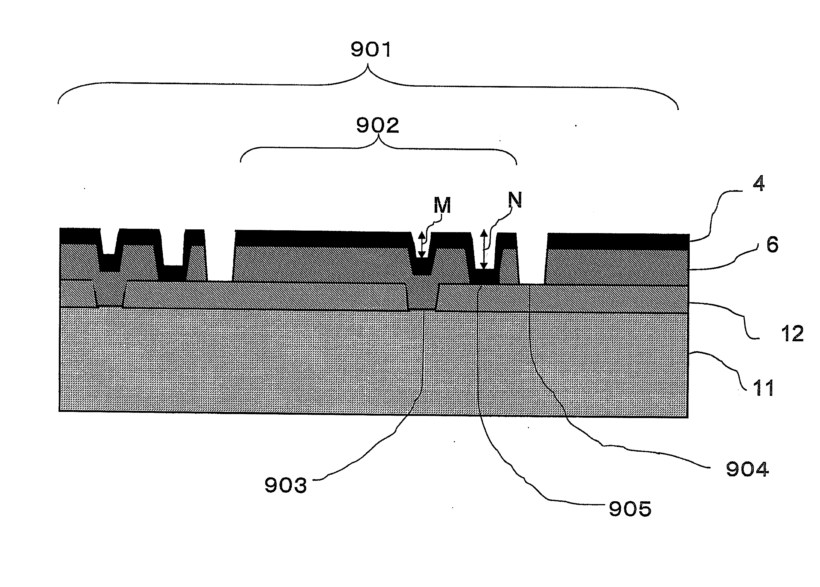
[0030]According to the present invention, in a thin film photoelectric conversion device, by a manufacturing method including a step of forming a transparent electrode layer and a step of forming a photoelectric conversion unit, a film thickness distribution of the transparent electrode layer is formed so as to be opposite to a film thickness distribution of the photoelectric conversion unit. Therefore, a haze ratio distribution is made to the extent of cancelling an influence of a transmittance distribution due to the film thickness distribution of the transparent electrode layer, and consequently, an in-plane distribution is generated in the light confinement effect, to improve a photoelectric characteristic inside the photoelectric conversion unit so as to improve a generation current of the entire thin film photoelectric conversion device. That is, the generation current of the thin film photoelectric conversion device is averaged in the substrate plane, while an entire generation current also increases, to improve conversion efficiency of the thin film photoelectric conversion device. This effect is exerted regardless of the presence or absence of serial connection.
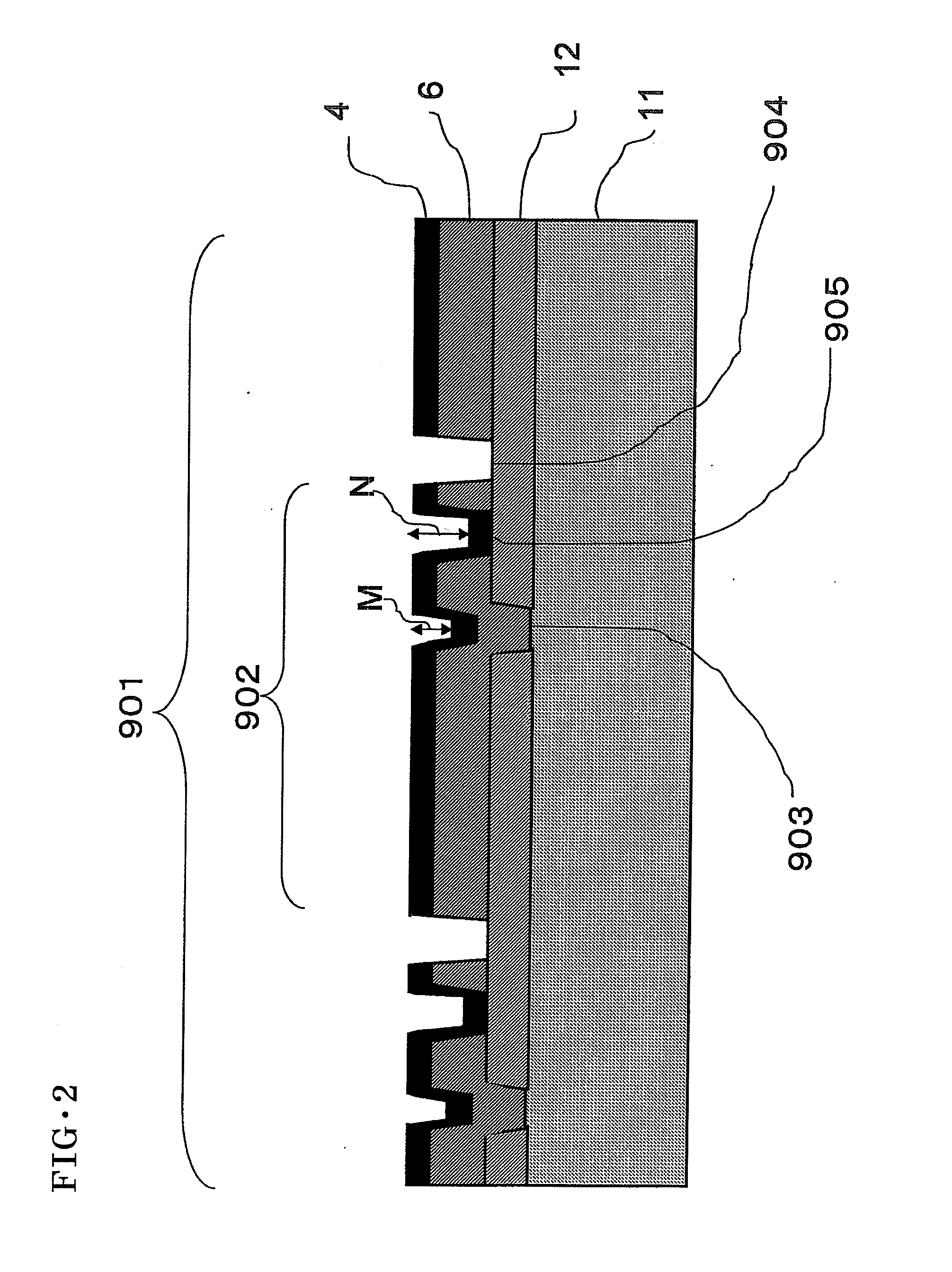
[0032]That is, according to the present invention, a film thickness distribution of the transparent electrode layer is formed so as to be opposite to a film thickness distribution of the photoelectric conversion unit in the integrated-type thin film photoelectric conversion device, whereby a haze ratio distribution is made, and consequently, an in-plane distribution is generated in the light confinement effect. As a result, a current value generated in each of the connected-in-series solar cells approaches a constant value so that output characteristics can be improved.

Problems solved by technology

Consequently, in the case of the integrated-type thin film photoelectric conversion device, the current value generated in each serially connected solar cell is not constant, and there occurs a problem in that a serially structured photoelectric conversion device is limited by a small current value and thus is unable to obtain sufficient output characteristics as a whole.

Method used


Image

  • Thin film photoelectric conversion device and method for manufacturing the same
  • Thin film photoelectric conversion device and method for manufacturing the same
  • Thin film photoelectric conversion device and method for manufacturing the same

Examples


reference example 1

[0149]As Reference Example 1, a thin film photoelectric conversion device 1 was produced. Specifically, on the transparent substrate 1 as a glass substrate of 125×125 mm and 4 mm in thickness, the transparent electrode layer 12 made of ZnO was formed by a low-pressure thermal CVD method. Heaters of low-pressure CVD device used are arranged as shown in FIG. 5, W0 is 600 mm, and L0 is 500 mm. The substrate was placed on the heater H6 at the center, and the transparent electrode layer 12 was formed. This transparent electrode layer 12 was formed with substrate temperatures T1 to T6 being 150° C., a pressure being 30 Pa, a flow rate of evaporated diethyl zinc being 200 sccm, a flow rate of evaporated water being 700 sccm, a flow rate of diborane (B2H6) being 2 sccm, and a flow rate of hydrogen being 1000 sccm. An average of film thicknesses Zt of the transparent electrode layer was 1661 nm, a deviation of the film thickness was ±3.9%, and a distribution thereof was uniform. Further, a h...

reference example 2

[0150]As Reference Example 2, the substrate 1 for a thin film photoelectric conversion device was produced in a similar manner as in Reference Example 1. However, the difference from Reference Example 1 is that film formation time was adjusted longer in order to change a film thickness. An average of film thicknesses Zt of this transparent electrode layer was 1837 nm, and a haze ratio was 33.0%.

reference example 3

[0151]As Reference Example 3, the substrate 1 for a thin film photoelectric conversion device was produced in a similar manner as in Reference Example 1. However, the difference from Reference Example 1 is that film formation time was adjusted longer than in Reference Example 2 in order to change a film thickness. An average of film thicknesses Zt of this transparent electrode layer was 1907 nm, and a haze ratio was 35.4%.


PUM

PropertyMeasurementUnit
Areaaaaaaaaaaa
Fractionaaaaaaaaaa
Current densityaaaaaaaaaa

Abstract

Provided is a thin film photoelectric conversion device with maximized output characteristic, by improving an uneven current value of a photoelectric conversion cell caused by an uneven film thickness and an uneven film quality of a photoelectric conversion semiconductor layer, which may be generated in scaling up an integrated-type thin film photoelectric conversion device. The thin film photoelectric conversion device includes: a substrate, a transparent electrode layer, a photoelectric conversion unit, and a back electrode layer. An increasing rate ΔZt of the film thickness Zt of the transparent electrode layer along X and an increasing rate ΔZs of the film thickness Zs of the photoelectric conversion unit along X have different signs, whereas one line segment in a parallel direction to a main surface of the substrate is taken as X″.

Description

TECHNICAL FIELD[0001]The present invention relates to a thin film photoelectric conversion device.BACKGROUND ART[0002]In recent years, among photoelectric conversion devices, a thin film photoelectric conversion device that needs fewer raw materials has attracted attention and its development has been vigorously made in order to achieve both lower cost and higher efficiency of photoelectric conversion devices including solar cells. In particular, a method for forming a satisfactory semiconductor layer on a low-priced substrate such as glass by means of a low-temperature process has been expected as a method capable of realizing low cost.[0003]Generally, in forming a superstrate-type thin film photoelectric conversion device, it is essential that a transparent electrode layer be provided in a part of the conversion device. The thin film photoelectric conversion device includes one or more photoelectric conversion units between the transparent electrode layer and a back electrode laye...

Claims


Application Information

Patent Timeline
IPC IPC(8): H01L31/0224H01L27/142H01L31/18
CPCC23C16/407C23C16/46H01L31/022466H01L31/035281H01L31/03921H01L31/0352H01L31/076H01L31/1804H01L31/1884Y02E10/548Y02E10/547H01L31/075H01L31/022425H01L31/022483H01L31/046Y02P70/50
Inventor FUJIBAYASHI, TAKASHISASAKI, TOSHIAKITAWADA, YUKO
Owner KANEKA CORP
Why Eureka
Try Eureka