Reducing cross-talk in high speed ceramic packages using selectively-widened mesh

Inactive Publication Date: 2011-03-17
LENOVO ENTERPRISE SOLUTIONS SINGAPORE
View PDF9 Cites 22 Cited by
  • Summary
  • Abstract
  • Description
  • Claims
  • Application Information

AI Technical Summary

Benefits of technology

[0007]One embodiment of the present invention provides a multi-layered ceramic package. The ceramic package includes a ceramic substrate, a signal layer having a plurality of signal lines in the ceramic substrate, and a mesh reference layer parallel to the signal layer. The mesh reference layer includes a plurality of intersecting reference lines of varying reference-line width in the plane of the mesh reference la

Problems solved by technology

An increase in both signal speeds and the proximity of signal lines has increased the potential for undesirable cross-talk between the signal

Method used


Image

  • Reducing cross-talk in high speed ceramic packages using selectively-widened mesh
  • Reducing cross-talk in high speed ceramic packages using selectively-widened mesh
  • Reducing cross-talk in high speed ceramic packages using selectively-widened mesh

Examples


Embodiment Construction

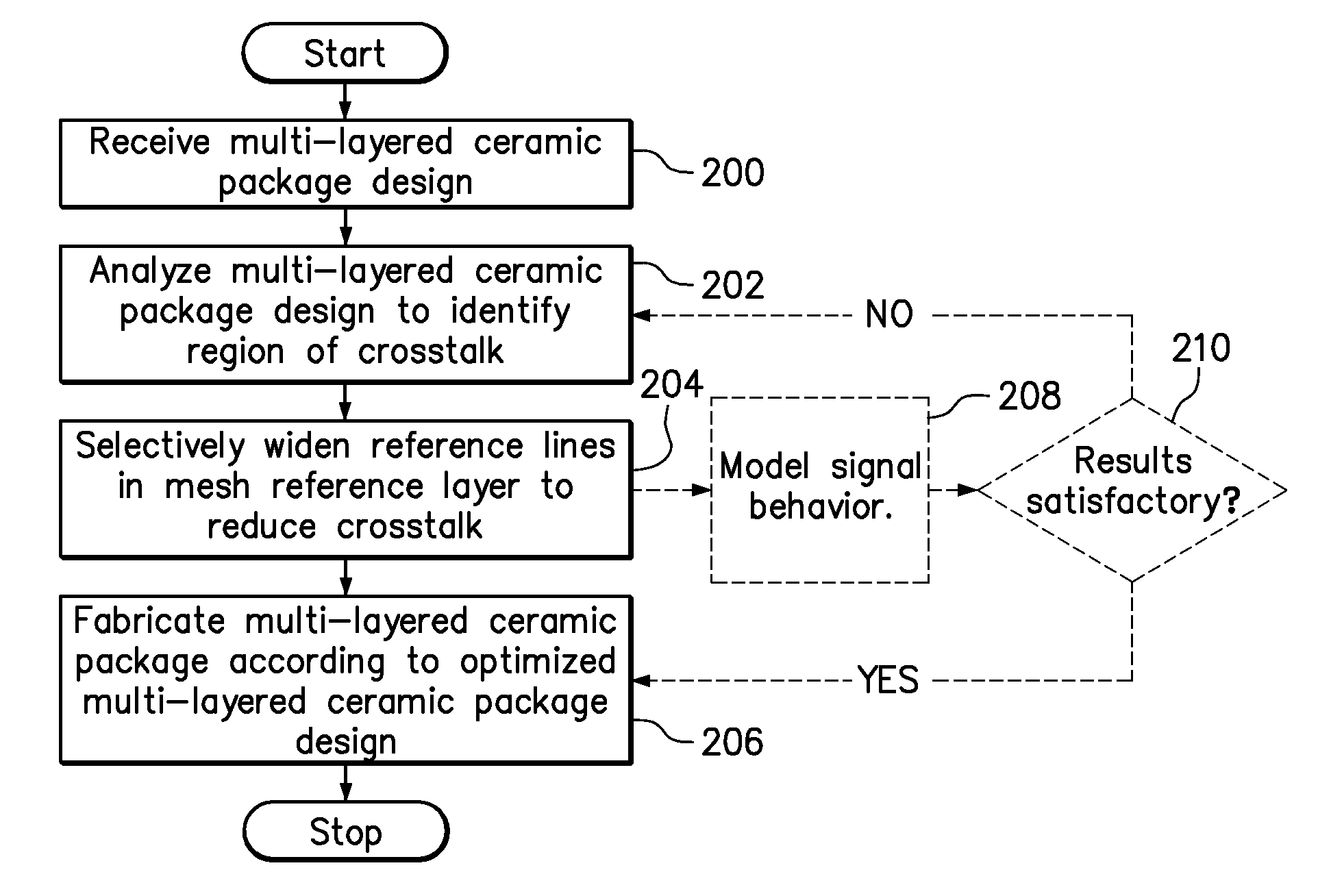
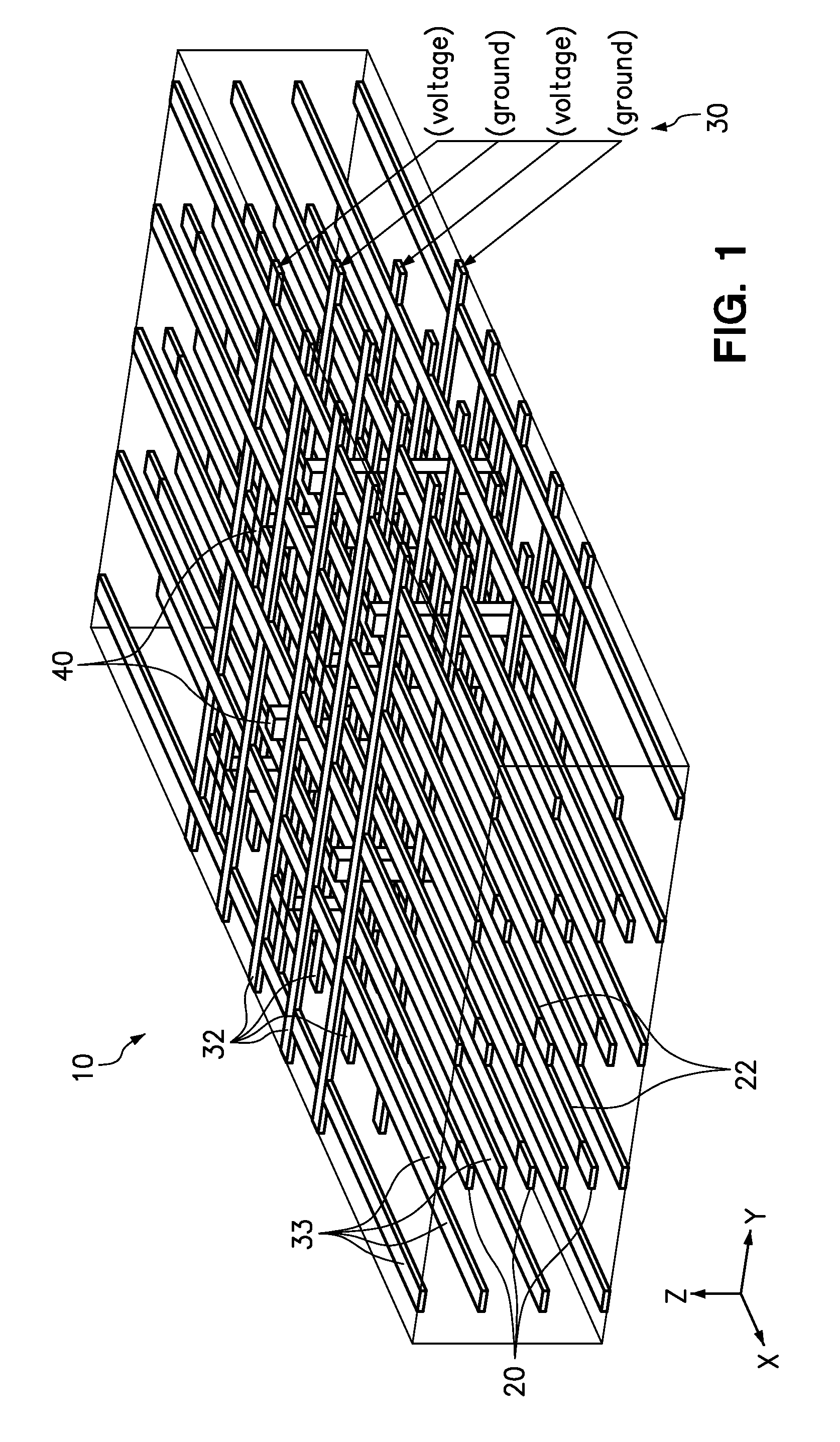
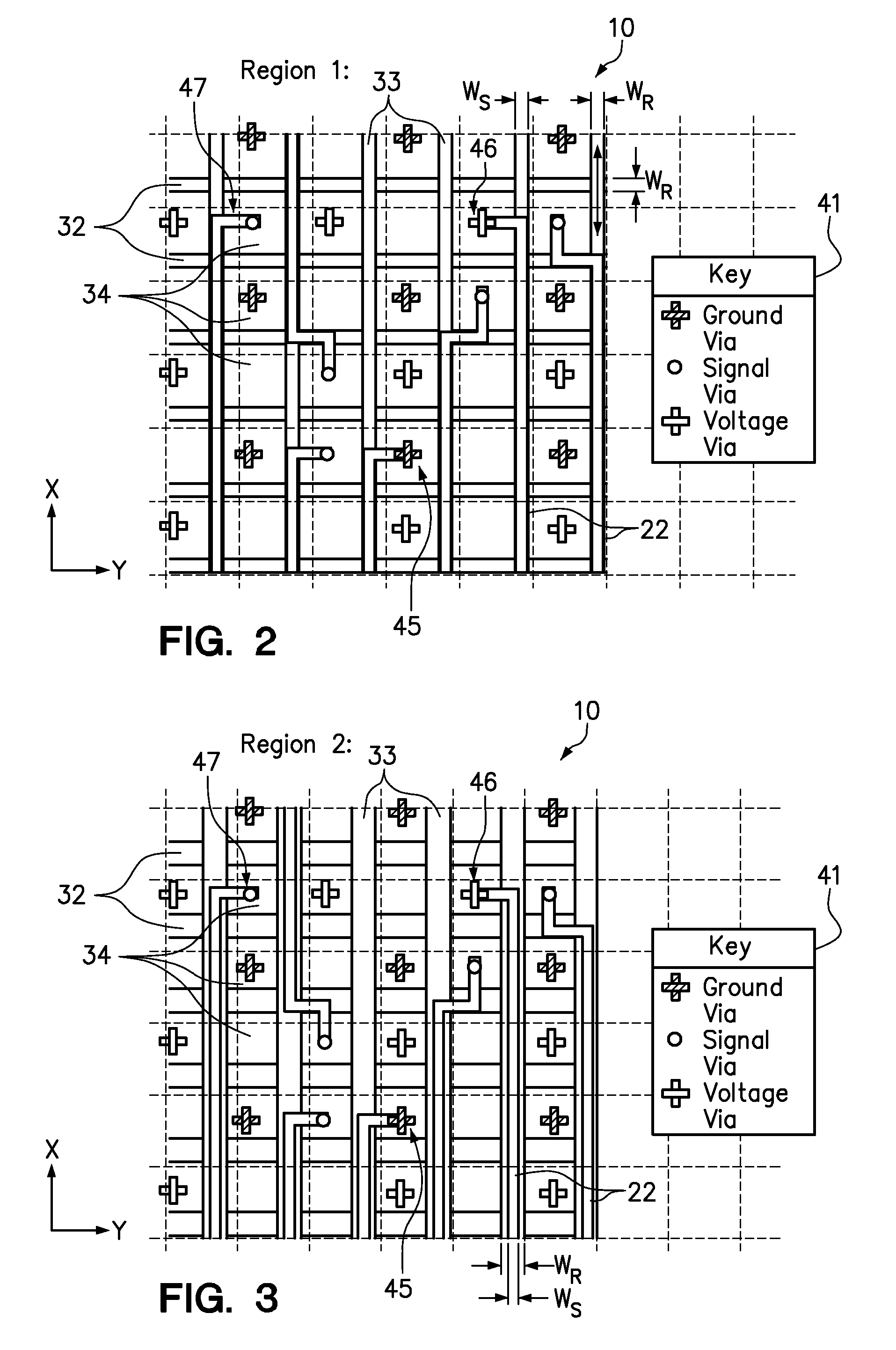
[0019]Embodiments of the invention include a multi-layered ceramic package, wherein the mesh reference lines in a mesh reference layer are selectively widened in areas having the greatest potential for signal cross-talk. As a result, cross-talk is effectively reduced in selected regions having a higher probability of cross-talk, without compromising the overall structural integrity of the entire ceramic package. In one embodiment, the mesh reference layers in a multi-layered ceramic package are alternating positive and ground reference layers, with signal layers sandwiched between the reference layers. Signal lines in the signal layer are aligned with the mesh reference lines, except where the signal lines traverse an opening between intersecting longitudinal and lateral mesh reference lines. Vias are used to tie in signal lines with selected mesh reference lines in vertically-spaced reference layers or signal lines in other signal layers. The reference lines are widened subject to ...


PUM

PropertyMeasurementUnit
Lengthaaaaaaaaaa
Lengthaaaaaaaaaa
Fractionaaaaaaaaaa

Abstract

One embodiment of the invention provides a multi-layered ceramic package. The ceramic package includes a signal layer having a plurality of signal lines and a mesh reference layer parallel to the signal layer. The mesh reference layer includes a plurality of intersecting reference lines of varying reference-line width in the plane of the mesh layer. The mesh reference lines may be widened in locations of probable signal cross-talk. Other embodiments of the invention include software for optimizing a ceramic package design by selectively widening mesh lines in regions of probable cross-talk, and systems for designing and manufacturing such a ceramic package.

Description

BACKGROUND[0001]1. Field of the Invention[0002]The present invention relates to integrated circuits, and more specifically to multi-layered ceramic packages.[0003]2. Background of the Related Art[0004]An integrated circuit (IC), also commonly referred to as a “microchip” or “chip,” is an electronic circuit comprising miniaturized semiconductor devices formed in a semiconductor substrate. Many copies of a chip may be formed on a large semiconductor wafer and then cut into individual chips, which may be interchangeably referred to in the art as “die chips” or simply “dies.” Semiconductor materials such as silicon are brittle, so an individual die chip is commonly packaged on a carrier to form a chip carrier, also known as a “chip package” or simply “package.” The carrier protects the fragile chip, in addition to providing an electrical and mechanical interface between the chip and a printed circuit board (PCB).[0005]A ceramic package is a type of package popular in a wide range of app...

Claims


Application Information

Patent Timeline
IPC IPC(8): H05K1/00G06F17/50H05K3/00
CPCG06F17/5036G06F17/5081G06F2217/82H05K1/0224Y10T29/49155H05K2201/09681H05K2201/09727H05K2201/09972H05K3/4629G06F30/398G06F30/367G06F2119/10
Inventor MUTNURY, BHYRAVCHOI, JINWOOCASES, MOISESNA, NANJU
Owner LENOVO ENTERPRISE SOLUTIONS SINGAPORE
Why Eureka
Try Eureka