Inspection system using back side illuminated linear sensor

a linear sensor and inspection system technology, applied in the field of optical imaging, can solve the problems of not being able to achieve full optimization, devices can also be susceptible to long-term ultra-violet and deep ultra-violet light damage, and techniques and performance compromises have been attempted, so as to achieve manageable power dissipation

Inactive Publication Date: 2011-03-31
KLA TENCOR TECH CORP
View PDF14 Cites 82 Cited by
  • Summary
  • Abstract
  • Description
  • Claims
  • Application Information

AI Technical Summary

Benefits of technology

[0014]Applying two constant voltages along the entire opposite edges of the gate region causes electrons to advance within each pixel toward an accumulation region. The advancing is enhanced by a nearly uniform and continuous electric field from the applied gate voltages. The conductivity of the gate can be chosen to maintain electric field uniformity while minimizing the current required and thus keeping power dissipation to manageable levels. Polysilicon gates may be doped or overcoated with conducting materials to achieve the required conductivity.
[0015]According to a second aspect of the present design, there is provided a method of inspecting specimens using a sensor comprising an array of linearly aligned pixels. The method comprises orienting each pixel and configuring the sensing device such that light energy reflected from a specimen is received at a back-side of said device and is collected in a pixel potential well near the front side of the device. Applying a plurality of constant voltages in stair-step fashion across regions of each pixel then causes electrons to advance or drift within each pixel toward an accumulation. The advancing is enhanced by transverse electric fields from the applied gate voltages.

Problems solved by technology

Such a configuration, known as front-illuminated, can be problematic because the resulting surface cannot generally be fully optimized for both optical performance, including high, stable quantum efficiency, and electrical performance, such as high speed and efficient, stable charge transport.
Such devices can also be susceptible to long-term ultra-violet and deep ultra-violet light damage, particularly in high sustained data-rate applications (heavy use conditions).
Various design techniques and performance compromises have been attempted but have not solved all of the issues.
The pixel size or aspect ratio can limit the operating speed of a linear sensor.
This can result in a phenomenon called image lag, which reduces the sensor performance in high-speed inspection applications.
In DUV applications, where the front-illuminated pixel cannot be covered with a gate, it is difficult to provide a potential variation within the pixel over a large region.
Lack of effective anti-blooming capability can make linear sensors unsuitable for high-speed darkfield ultra-violet darkfield inspection applications.

Method used


Image

  • Inspection system using back side illuminated linear sensor
  • Inspection system using back side illuminated linear sensor
  • Inspection system using back side illuminated linear sensor

Examples


Embodiment Construction

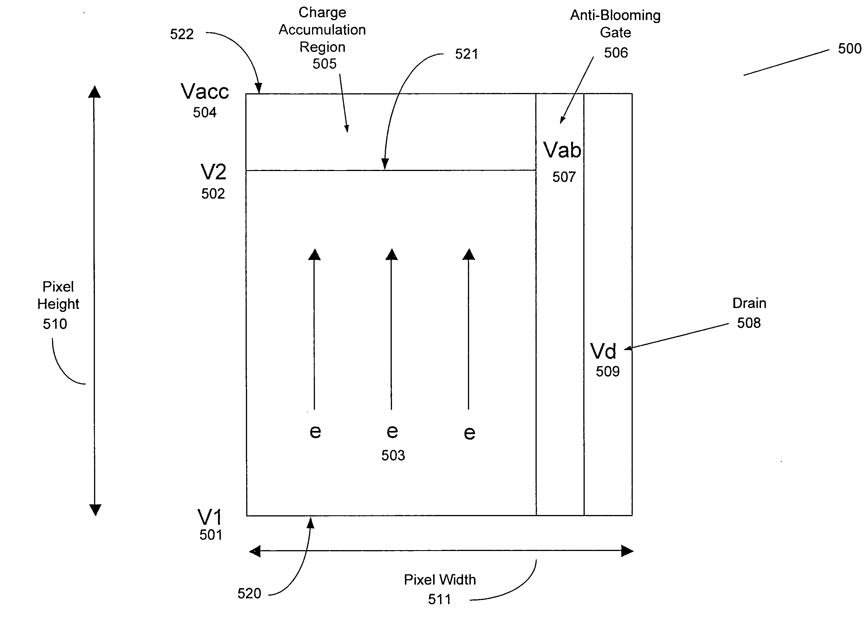
[0024]According to the present invention, there is provided an inspection system comprising a back side illuminated linear sensing arrangement that employs one or more gates over the exposure region to facilitate control of the voltage profile across the exposed area. The design orients each pixel and configures the sensing device such that light energy reflected from a specimen is received at a back-side of the sensing device and is collected in a pixel potential well near the front side of the device. Applying a plurality of constant voltages in stair-step fashion across regions of each pixel then causes electrons to advance or drift within each pixel toward an accumulation region or zone. Advancing is enhanced by transverse electric fields from the applied gate voltages.

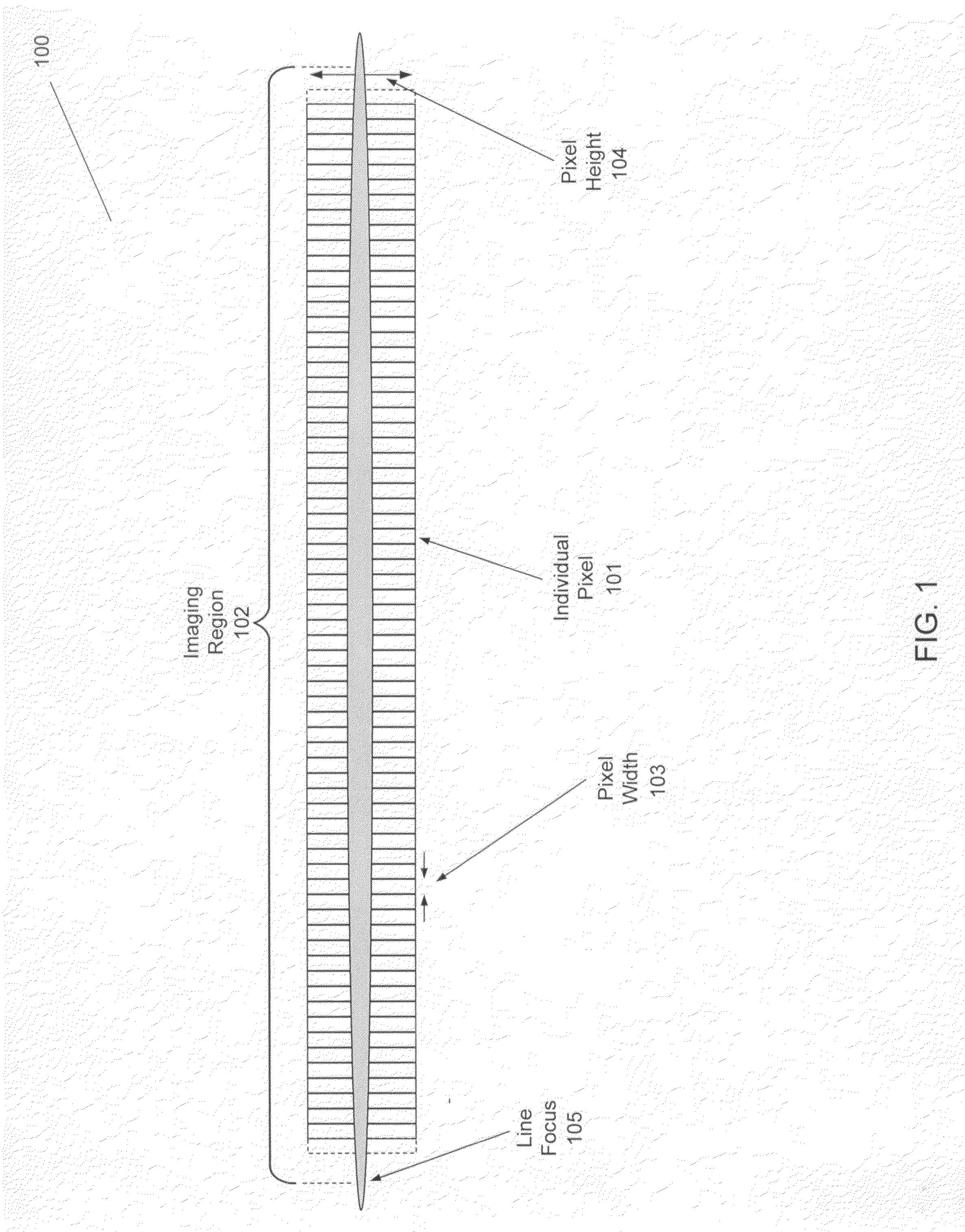
[0025]The design is particularly applicable to inspection and metrology systems. The implementation is either a single gate implementation or multiple gate implementation producing in either case a continuous volt...


PUM

PropertyMeasurementUnit
oblique incidence angleaaaaaaaaaa
light energyaaaaaaaaaa
voltageaaaaaaaaaa

Abstract

An improved inspection system using back-side illuminated linear sensing for propagating charge through a sensor is provided. Focusing optics may be used with a back side illuminated linear sensor to inspect specimens, the back side illuminated linear sensor operating to advance an accumulated charge from one side of each pixel to the other side. The design comprises controlling voltage profiles across pixel gates from one side to the other side in order to advance charge between to a charge accumulation region. Controlling voltage profiles comprises attaching a continuous polysilicon gate across each pixel within a back side illuminated linear sensor array. Polysilicon gates and voltages applied thereto enable efficient electron advancement using a controlled voltage profile.

Description

BACKGROUND OF THE INVENTION[0001]1. Field of the Invention[0002]The present invention relates generally to the field of optical imaging and more specifically to optical systems for microscopic imaging, inspection and lithography applications.[0003]2. Description of the Related Art[0004]Many optical systems and electronic systems have an ability to inspect or image features on the surface of a specimen to determine defects. Specimens may include semiconductor wafers or photomasks and partially fabricated integrated circuits. Defects on such specimens may be relatively small in size and can take the form of imperfections randomly localized on the specimen surface, such as particles, scratches, process variations, repeating pattern defects, and so forth. Such defects are typically seven or more orders of magnitude smaller than the wafer itself.[0005]Techniques and devices for inspecting specimens for these microscopic defects are generally available in the art and are embodied in vario...

Claims


Application Information

Patent Timeline
Patent Type & Authority Applications(United States)
IPC IPC(8): H01L31/00G01N21/00
CPCG01N21/9501G01N2021/95676G01N2021/8822G01N21/95623
Inventor ARMSTRONG, J. JOSEPHCHUANG, YUNG-HOBROWN, DAVID L.
Owner KLA TENCOR TECH CORP
Why Eureka
Try Eureka