Semiconductor Device

a semiconductor device and silicon technology, applied in the direction of semiconductor devices, electrical devices, transistors, etc., can solve the problems of cmos semiconductor device damage, voltage reaching the gate oxide film breakdown before the surface breakdown, etc., and achieve the effect of easy setting a holding

Inactive Publication Date: 2011-04-07
EBIHARA MIKA +1
View PDF2 Cites 3 Cited by
  • Summary
  • Abstract
  • Description
  • Claims
  • Application Information

AI Technical Summary

Benefits of technology

[0006]It is an object of the present invention to provide an electrostatic protective element capable of arbitrarily setting an operating voltage (trigger voltage) and a holding voltage at a low level, which has not been achieved in a conventional electrostatic protective circuit using an NMOS transistor having a conventional drain structure, with a small occupation area at low cost.
[0008]According to the present invention, a P-type impurity is introduced in an electrostatic protective circuit using an NMOS transistor having a conventional drain structure, thereby making it possible to obtain an element capable of easily setting a holding. voltage with a trigger voltage at a low level, which has not been achieved in a conventional electrostatic protective circuit using an NMOS transistor having a conventional drain structure. As a result, it is possible to achieve an ESD protective circuit capable of protecting the CMOS transistor, in which the voltage is reduced, from the ESD, thereby obtaining a significant effect in a plurality of ICs.

Problems solved by technology

However, with the advancement in miniaturization of a semiconductor device and downsizing of an electronic device using the same, reductions in a voltage of the CMOS semiconductor device and in a thickness of a gate oxide film have been promoted, there arises a problem in that, in a conventional electrostatic protection circuit using an NMOS transistor having a conventional drain structure, voltage reaches the gate oxide film breakdown before the surface breakdown occurs, or the CMOS semiconductor device damages due to a static electricity before the electrostatic protective circuit operates.

Method used


Image

  • Semiconductor Device
  • Semiconductor Device
  • Semiconductor Device

Examples


first embodiment

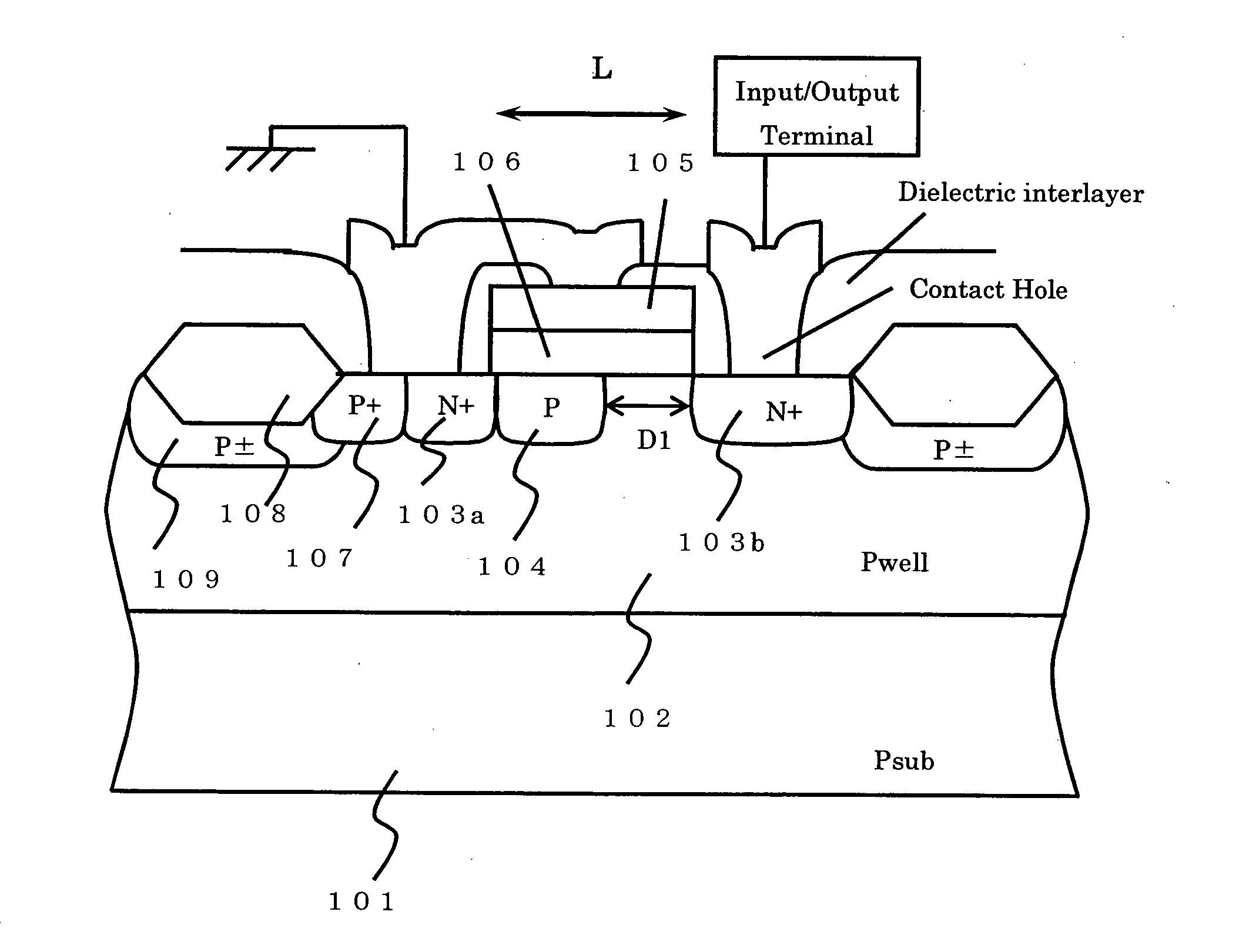
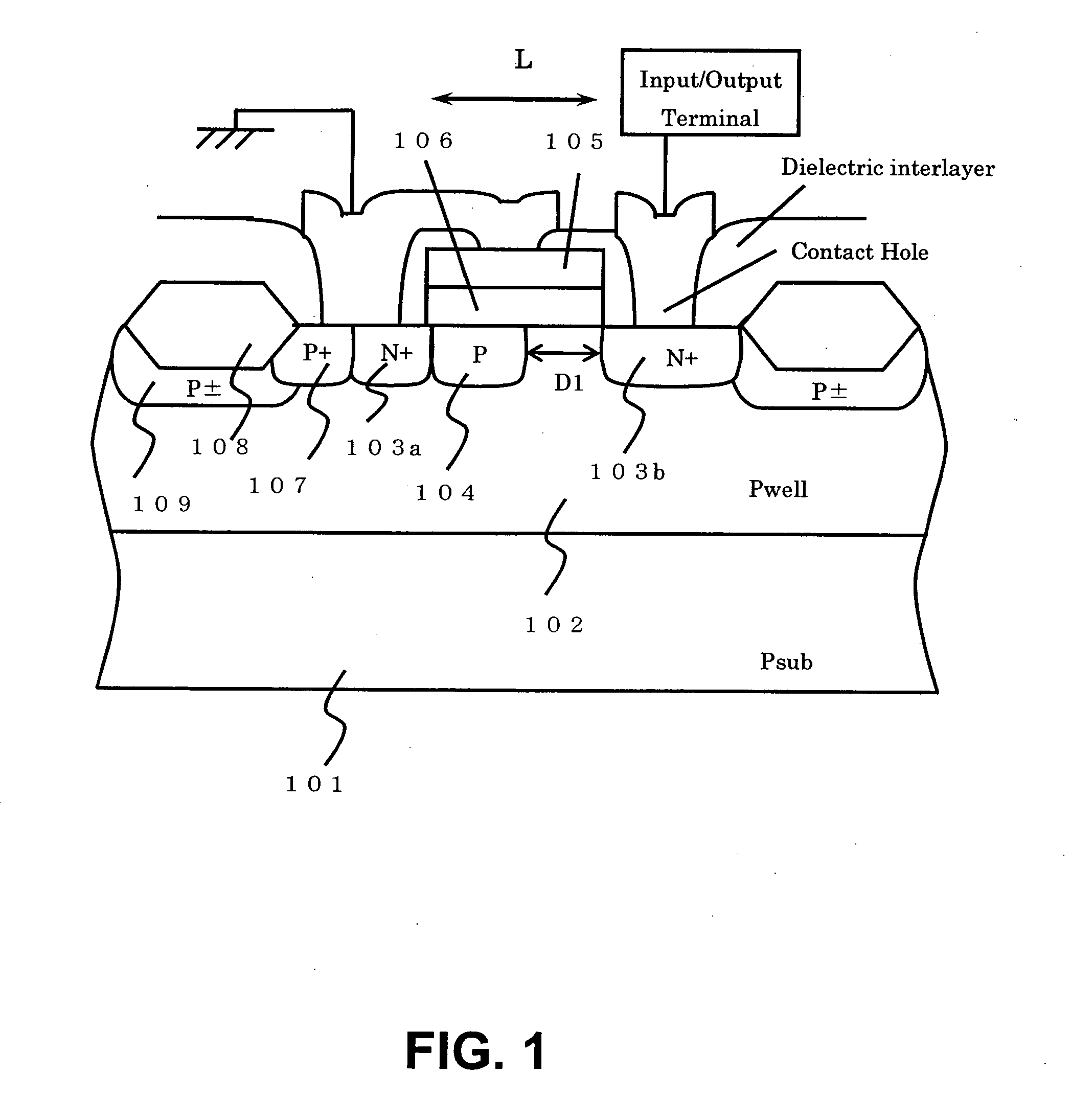
[0014]FIG. 1 is a schematic sectional diagram of an NMOS transistor having a conventional drain structure of a semiconductor device according to a first embodiment of the present invention.

[0015]The NMOS transistor includes a P-type well region 102 formed on a P-type silicon semiconductor substrate 101, a gate oxide film 106 and a polysilicon gate electrode 105 which are formed on the P-type well region 102, a P-type diffusion layer 104 having a high concentration which is formed to contact with the source region locally between an N-type source diffusion layer 103a and an N-type drain diffusion layer 103b, which are formed on a surface of a silicon substrate at both ends of the gate electrode and have a high concentration, and a P-type diffusion layer 107 which is provided so as to take a potential of the P-type well region 102, and has a high concentration. N-type drain diffusion layer 103b is connected to an input / output terminal through wiring, and the N-type source diffusion la...

second embodiment

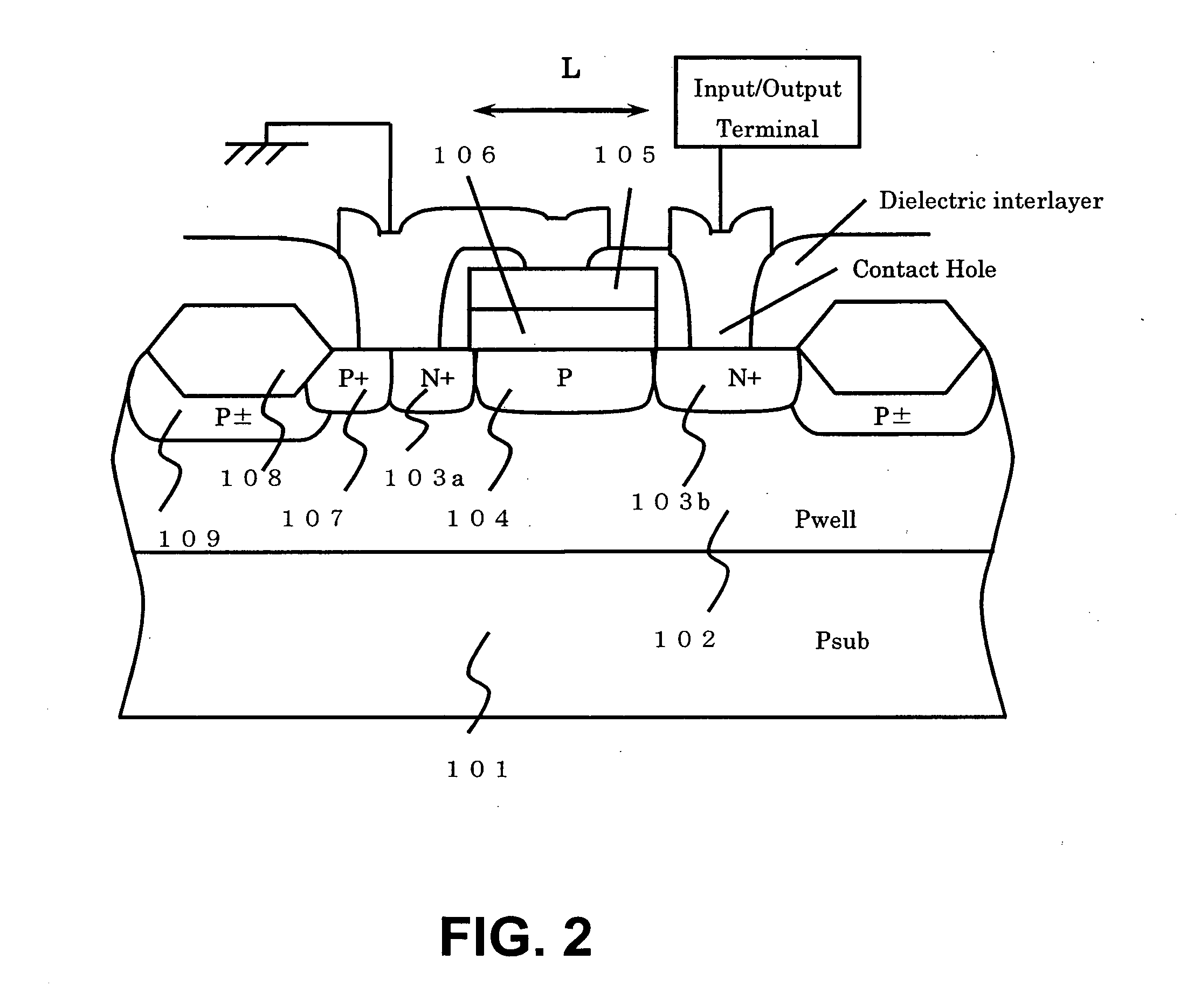
[0020]FIG. 2 is a schematic sectional diagram of an NMOS transistor having a conventional drain structure of a semiconductor device according to a second embodiment of the, present invention.

[0021]As shown in FIG. 2, a P-type diffusion layer may be formed on an entire area provided immediately below a gate between N-type source and drain diffusion layers.


PUM


Abstract

Provided is a semiconductor device capable of easily setting a holding voltage with a low trigger voltage by locally forming a P-type diffusion layer between N-type source and drain diffusion layers of an NMOS transistor having a conventional drain structure used as an electrostatic protective element of the semiconductor device.

Description

BACKGROUND OF THE INVENTION[0001]1. Field of the Invention[0002]The present invention relates to a semiconductor device, and more particularly, to a semiconductor device used for preventing damage due to a static electricity to a CMOS semiconductor device.[0003]2. Description of the Related Art[0004]Up to now, in a CMOS semiconductor device, as an electrostatic discharge (hereinafter, referred to as “ESD”) protective element, an NMOS transistor having a conventional drain structure in which a gate electrode is held to a substrate potential as shown in FIG. 3 is used in many cases. The operation principle of this transistor is that surface breakdown of the transistor, which takes place in the voltage range between the maximum operating voltage of the CMOS semiconductor device and a voltage which does not cause breakdown in a standard NMOS transistor, triggers current flow between the drain 103b and the P-type substrate 101 to increase the potential of the substrate 101, causing a for...

Claims


Application Information

Patent Timeline
Patent Type & Authority Applications(United States)
IPC IPC(8): H01L29/78
CPCH01L27/0266H01L29/0638H01L29/861H01L29/105H01L29/1083H01L29/1045
Inventor EBIHARA, MIKARISAKI, TOMOMITSU
Owner EBIHARA MIKA
Why Eureka
Try Eureka