Plasma reactor for abating hazardous materials and driving method thereof

US20110089017A1Active Publication Date: 2011-04-21KOREA INST OF MASCH & MATERIALS

Image

  • Plasma reactor for abating hazardous materials and driving method thereof
  • Plasma reactor for abating hazardous materials and driving method thereof
  • Plasma reactor for abating hazardous materials and driving method thereof

Examples


Embodiment Construction

[0042]The present invention will be described more fully hereinafter with reference to the accompanying drawings, in which exemplary embodiments of the invention are shown. As those skilled in the art would realize, the described embodiments may be modified in various different ways, all without departing from the spirit or scope of the present invention.

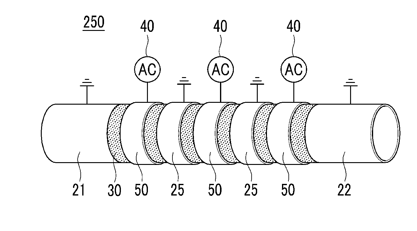
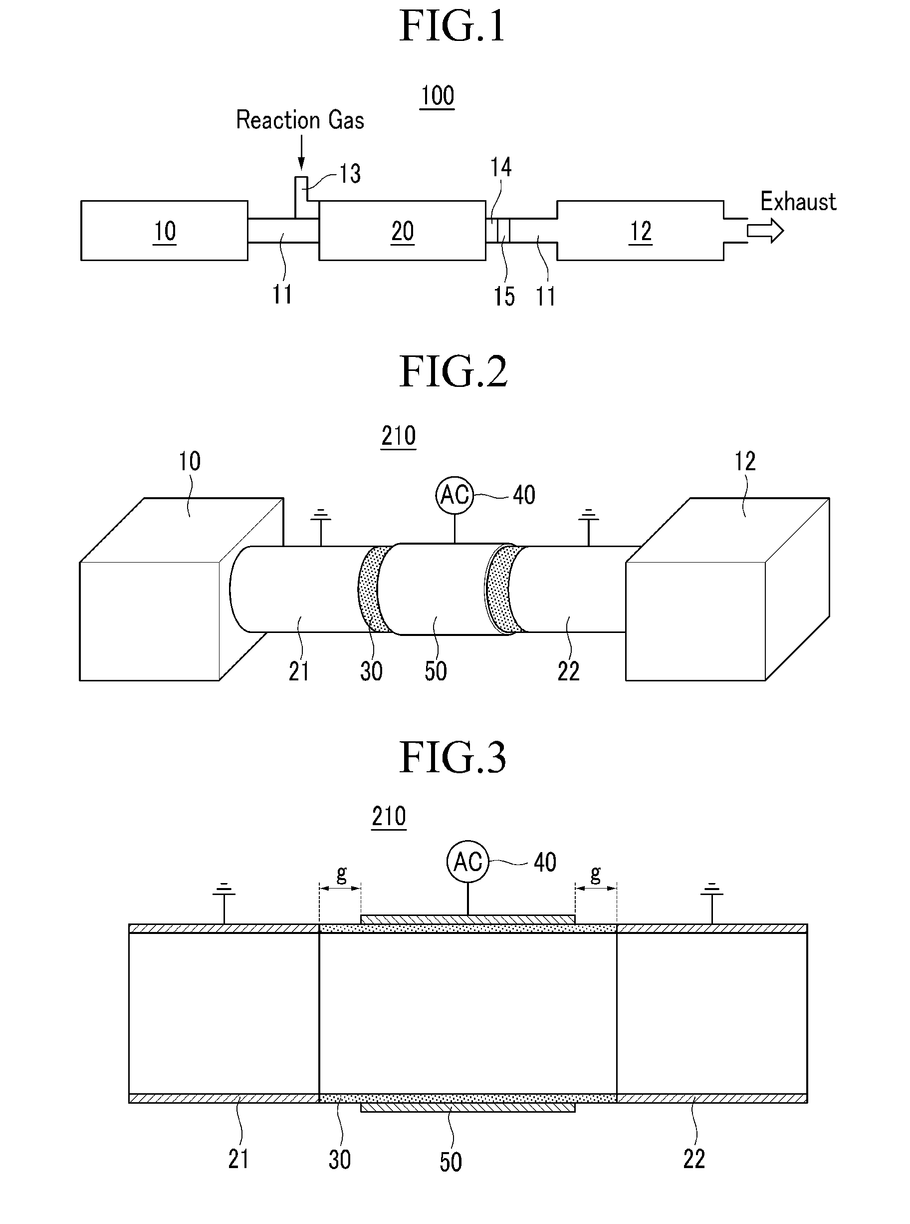
[0043]FIG. 1 is a configuration diagram of a low-voltage process system including a plasma reactor. The low-pressure process system of FIG. 1 may be applied to a process for manufacturing a display or a semiconductor.

[0044]Referring to FIG. 1, the low pressure process system 100 includes a low pressure process chamber 10, a vacuum pump 12 connected to the low pressure process chamber 10 through a joint pipe 11, and a plasma reactor 20 mounted in the joint pipe 11. The plasma reactor 20 is installed in front of the vacuum pump 12 and the inside thereof maintains a low pressure state similar to the low pressure process chamber 10. A r...


PUM


Abstract

The present invention provides a plasma reactor for abating hazardous materials generated in a low-pressure process during a process of manufacturing a display or a semiconductor. A plasma reactor for abating hazardous materials according to an exemplary embodiment of the present invention includes: a first ground electrode and a second ground electrode disposed at a distance from each other; a dielectric fixed between the first ground electrode and the second ground electrode; and at least one driving electrode disposed on an outer surface of the dielectric, being spaced apart from the first ground electrode and the second ground electrode and connected to an AC power supply unit to receive a driving voltage therefrom.

Description

CROSS-REFERENCE TO RELATED APPLICATION[0001]This application claims priority to and the benefit of Korean Patent Application Nos. 10-2009-0098892 and 10-2010-0091074 filed in the Korean Intellectual Property Office on Oct. 16, 2009 and Sep. 16, 2010, the entire contents of which are incorporated herein by reference.FIELD OF THE INVENTION[0002]The present invention relates to a plasma reactor for abating hazardous materials, and more particularly, to a plasma reactor for abating hazardous materials generated during a low-pressure process chamber among processes for manufacturing a display or a semiconductor.BACKGROUND OF THE INVENTION[0003]Among processing for manufacturing a display or a semiconductor, ashing, etching, depositing, cleaning, nitriding processes, or the like, are performed in a low-pressure process chamber. As gas used in the low-pressure process, there are (1) volatile organic compound (trichloroethylene, 1,1,1-trichloroethane, methanol, acetaldehyde, or the like), (...

Claims


Application Information

Patent Timeline
21 Apr 2011
Publication
US20110089017A1
IPC
B01J19/12; B01J19/08
CPC
H01J37/32541; H05H2245/1215; Y02C20/30; B01D53/323; H01J37/32091; H01J37/32348; H01J37/32834; H01J37/32844
Inventors
HUR, MIN; CHA, MIN-SUK