Semiconductor device

Inactive Publication Date: 2011-04-21
SEMICON ENERGY LAB CO LTD
View PDF31 Cites 312 Cited by
  • Summary
  • Abstract
  • Description
  • Claims
  • Application Information

AI Technical Summary

Benefits of technology

[0023]A combination of a transistor using a material other than an oxide semiconductor and a transistor using an oxide semiconductor allows for the production of a semiconductor device requiring electric characteristics different from those of transistors using an oxide semiconductor (e.g. difference in carriers characteristics, which have an effect on the behavior of the element).
[0024]Further, a transistor using an oxide semiconductor has good switching characteristics, so that an exce

Problems solved by technology

However, semiconductor devices using silicon or the like do not have adequate switching characteristics; e.g. a problem is that a semiconductor device is damaged by a significantly high flow-through current in the case of the fabrication of a CMOS inverter circuit and that the power consumption is increased by a significantly high flow-through current.
Therefore, a flow of

Method used


Image

  • Semiconductor device
  • Semiconductor device
  • Semiconductor device

Examples


embodiment 1

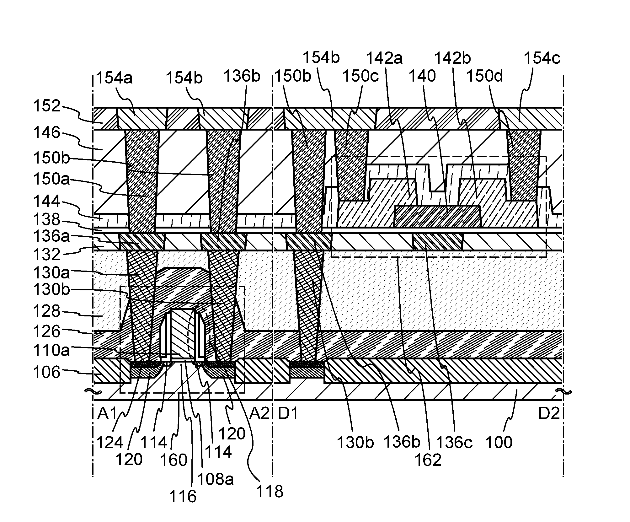
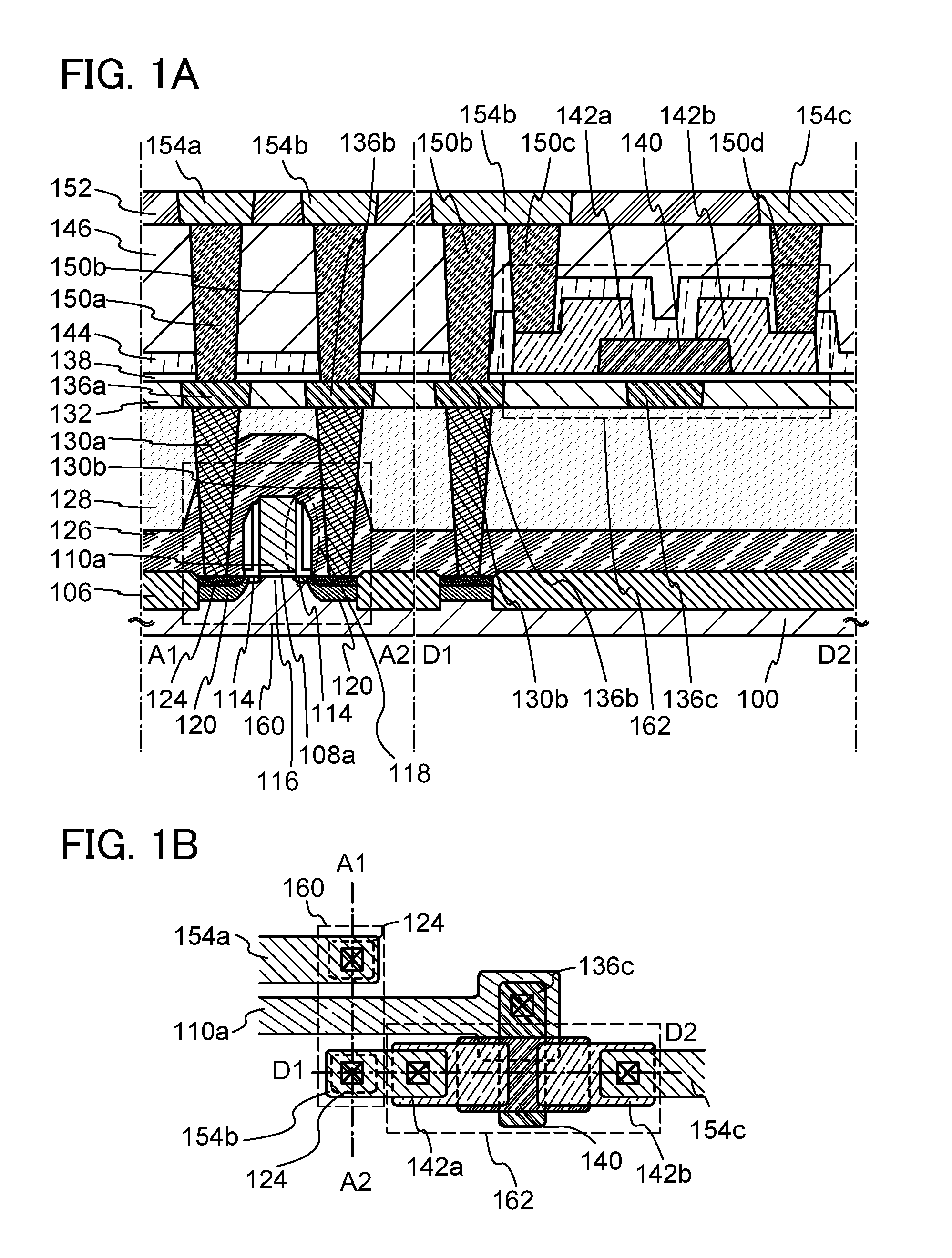
[0039]In this embodiment, the structure and the manufacturing method of a semiconductor device according to one embodiment of the present invention will be described with reference to FIGS. 1A and 1B, FIG. 2, FIGS. 3A and 3B, FIGS. 4A to 4H, FIGS. 5A to 5G, and FIGS. 6A to 6D.

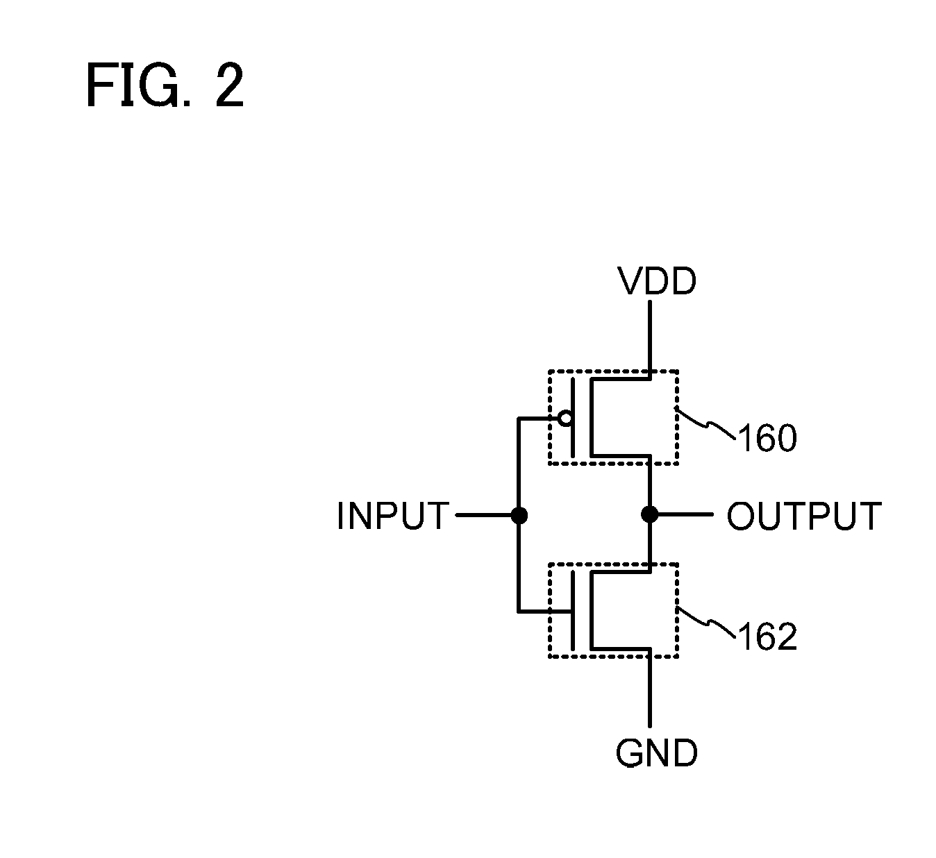
[0040]FIG. 1A shows a cross-sectional view of the semiconductor device according to this embodiment. FIG. 1B shows a plane view of the semiconductor device according to this embodiment. Here, FIG. 1A corresponds to section A1-A2 and D1-D2 shown in FIG. 1B. The semiconductor device shown in FIGS. 1A and 1B includes a p-type transistor 160 in its lower part and an n-type transistor 162 using an oxide semiconductor in its upper part.

[0041]The p-type transistor 160 includes a channel formation region 116 in a substrate 100 containing a semiconductor material; impurity regions 114 and heavily doped regions 120, a combination of the impurity regions 114 and the heavily doped regions 120 can simply be referred to as i...

embodiment 2

[0129]In this embodiment, the structure of a semiconductor device according to another embodiment of the disclosed invention is described with reference to FIGS. 7A and 7B and FIG. 8. Note that in this embodiment, the structure of a semiconductor device which can be used as a memory element is described.

[0130]FIG. 7A shows a cross-sectional view of a semiconductor device according to this embodiment. FIG. 7B shows a plane view of the semiconductor device according to this embodiment. Here, FIG. 7A shows section E1-E2 and section F1-F2 of FIG. 7B. The semiconductor device shown in FIGS. 7A and 7B includes a transistor 260 in its lower part, which is formed using a material other than an oxide semiconductor, and a transistor 262 in its upper part, which is formed using an oxide semiconductor.

[0131]The transistor 260 using a material other than an oxide semiconductor includes: a channel formation region 216 in a substrate 200 containing a semiconductor material, impurity regions 214 an...

embodiment 3

[0147]In this embodiment, the structure of a semiconductor device according to another embodiment of the disclosed invention is described with reference to FIGS. 9A and 9B and FIG. 10. Note that in this embodiment, the structure of a semiconductor device which can be used as a memory element is described.

[0148]FIG. 9A shows a cross-sectional view of a semiconductor device according to this embodiment. FIG. 9B shows a plane view of the semiconductor device according to this embodiment. Here, FIG. 9A shows section G1-G2 and section H1-H2 in FIG. 9B. The semiconductor device shown in FIGS. 9A and 9B includes, in its lower part, a p-type transistor 460 and an n-type transistor 464 which are formed using a material other than an oxide semiconductor, and includes, in its upper part, a transistor 462 using an oxide semiconductor.

[0149]The p-type transistor 460 and the n-type transistor 464 which are formed using a material other than an oxide semiconductor have a similar structure to that ...


PUM


Abstract

An objet of the present invention is to provide a semiconductor device with a new structure. Disclosed is a semiconductor device including a first transistor which includes a channel formation region on a substrate containing a semiconductor material, impurity regions formed with the channel formation region interposed therebetween, a first gate insulating layer over the channel formation region, a first gate electrode over the first gate insulating layer, and a first source electrode and a first drain electrode which are electrically connected to the impurity region; and a second transistor which includes a second gate electrode over the substrate containing a semiconductor material, a second gate insulating layer over the second gate electrode, an oxide semiconductor layer over the second gate insulating layer, and a second source electrode and a second drain electrode which are electrically connected to the oxide semiconductor layer.

Description

TECHNICAL FIELD[0001]The technical field of the present invention relates to a semiconductor device and a manufacturing method of the semiconductor device. Note that here, semiconductor devices refer to general elements and devices which function utilizing semiconductor characteristics.BACKGROUND ART[0002]There are a wide variety of metal oxides, and metal oxides have various applications. Indium oxide is a well-known material and has been used for transparent electrodes required in liquid crystal display devices or the like.[0003]Some metal oxides have semiconductor characteristics. Examples of metal oxides having semiconductor characteristics are tungsten oxide, tin oxide, indium oxide, zinc oxide, and the like. Thin film transistors having channel formation regions made of any of such metal oxides have already been described (e.g. see Patent Documents 1 to 4 and Non-Patent Document 1 etc.).[0004]Incidentally, not only single-component oxides but also multi-component oxides are kn...

Claims


Application Information

Patent Timeline
IPC IPC(8): H01L29/12
CPCH01L21/84H01L27/0688H01L29/7869H01L27/1225H01L27/1207
Inventor YAMAZAKI, SHUNPEIKOYAMA, JUNIMAI, KEITARO
Owner SEMICON ENERGY LAB CO LTD
Why Eureka
Try Eureka