Silicone rubber material for soft lithography

a technology of soft lithography and silicon rubber, which is applied in the field of silicon rubber like materials, can solve the problems of poor accommodation on rough and non-flat surfaces, subject to problems, and conventional pdms materials are susceptible to rounding of sharp corners, and achieves the effects of avoiding the disadvantages of high incubation temperatures, high incubation temperatures, and simple and inexpensive construction

Active Publication Date: 2011-04-28
KONINKLIJKE PHILIPS ELECTRONICS NV
View PDF8 Cites 17 Cited by
  • Summary
  • Abstract
  • Description
  • Claims
  • Application Information

AI Technical Summary

Benefits of technology

[0028]The method according to the invention is advantageous as it does not require high incubation temperatures; i.e. curing temperatures. Disadvantages associated with high incubation temperatures are thereby avoided. For example, high incubation temperatures may result in thermal mismatch between a master pattern material and the stamp material. This is due to the build up of large stresses during heating and cooling and may result in crack formation and damage of features.
[0029]A method according to the invention has the advantage that it is relatively simple, inexpensive and has a high reproducibility which makes it suitable for mass production. The stamp layers thus formed may be used in several types of stamp structures or patterning devices.

Problems solved by technology

Although such materials are capable of establishing reproducible conformal contact with a substrate material, they are subject to problems associated with pressure induced deformations when providing very small pattern features in the nanometer range, e.g. in the sub 100 nm range.
Moreover, conventional PDMS materials are susceptible to rounding of sharp corners due to surface tension, especially when features smaller than 100 nm are molded.
However, an increase in Young's modulus may result in that the material becomes too rigid, resulting in poor accommodation onto rough and non-flat surfaces.
Hence, soft lithography is limited in resolution by the stamp material used, and for large area imprint the material needs to have a Young's modulus being high enough to generate stable features having very small dimensions, but at the same time the material must be as soft as possible to accommodate conformal contact on rough and non-flat substrates.
A drawback in using silicone resins in transfer layers for lithographic purposes is that resins are glass like with glass transitioning temperatures ranging from room temperature to 300-400° C. The Young's modulus of such resin materials is very high (above 100-200 MPa), which may prevent conformal contact, as the stamp cannot follow the micrometer and even nanometer sized roughness of a substrate.
The imprinted layer forms a rigid material, and removing the stamp requires high forces.
This results in that the forces on the features in the stamp and imprinted features become very high, which may result in damage of the stamp and / or the imprinted features.

Method used


Image

  • Silicone rubber material for soft lithography
  • Silicone rubber material for soft lithography
  • Silicone rubber material for soft lithography

Examples


Embodiment Construction

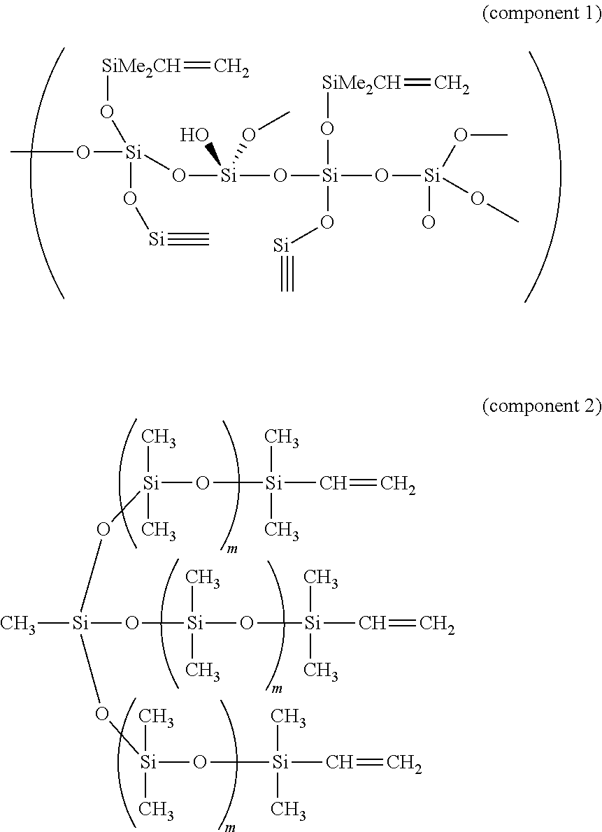
[0049]The present invention relates to a silicone rubber like material comprising at least one T branched and / or Q branched (poly)siloxane precursor crosslinked by at least one linear polysiloxane, wherein said material has a Young's modulus in the range of from 7 MPa to 80 MPa.

[0050]As used herein the term “T branched (poly)siloxane precursor” refers to a silicone material comprising a network of oligosiloxanes, wherein one or more silicone atoms are bound by at least three oxygen atoms to other silicone atoms. The term “Q branched (poly)siloxane precursor” refers to a silicone material comprising a network of oligosiloxanes, wherein one or more silicone atoms are bound by at least four oxygen atoms to other silicone atoms.

[0051]The T branched (poly)siloxane precursor is able to form 3-way branching chains, i.e. networks, when crosslinked by linear polysiloxanes, typically linear PDMS chains. Likewise, the Q branched (poly)siloxane precursor is able to form 4-way branching chains, ...


PUM

PropertyMeasurementUnit
Young's modulusaaaaaaaaaa
temperatureaaaaaaaaaa

Abstract

The present invention relates to a silicone rubber like material and a printing device including a stamp layer (100;201) comprising such a material. The material is suitable for use in soft lithography as it enables stable features having mensions in the nanometer range to be obtained on a substrate, and also allows for the accommodation onto rough and non-flat substrate surfaces. The invention also relates to methods for manufacturing the silicone rubber like material and stamp layer (100;201) and use thereof in lithographic processes.

Description

FIELD OF THE INVENTION[0001]The present invention relates to a silicone rubber like material and a stamp layer comprising such a material for use in soft lithography. The invention also relates to methods for manufacturing the silicone rubber like material and use thereof in lithographic processes and devices.BACKGROUND OF THE INVENTION[0002]In recent years, techniques for designing micrometer sized structures in electrical, optical and photonic applications have been developed. Such techniques may be based on molding and contact printing, collectively referred to as soft lithography.[0003]Soft lithography typically makes use of a patterning device, such as a stamp comprising a transfer surface having a well defined relief pattern. Structures and features are formed upon conformal contact between the stamp transfer surface and a substrate.[0004]In order to pattern large areas using soft lithography techniques, it is crucial that no deformation of the patterns occurs when the stamp i...

Claims


Application Information

Patent Timeline
Patent Type & Authority Applications(United States)
IPC IPC(8): B41F1/18B41N1/08
CPCB41C1/08B41N1/12B82Y10/00B82Y40/00C08G77/12C08G77/20G03F7/0002C08G77/80C08L83/04C08L83/00B29K2083/005Y10T428/24802B29C59/02
Inventor VERSCHUUREN, MARCUS ANTONIUS
Owner KONINKLIJKE PHILIPS ELECTRONICS NV
Why Eureka
Try Eureka