Organic electroluminescence element, display device and lighting device

a technology of electroluminescence element and display device, which is applied in the direction of thermoelectric device, luminescent composition, other domestic articles, etc., can solve the problems of insufficient accuracy during the production process of elements, poor utilization efficiency of materials, and increase in space, so as to minimize dark spots, improve light emission efficiency, and prolong service life

Active Publication Date: 2011-04-28
MERCK PATENT GMBH
View PDF10 Cites 21 Cited by
  • Summary
  • Abstract
  • Description
  • Claims
  • Application Information

AI Technical Summary

Benefits of technology

[0030]Employing the present invention, it has become possible to provide a multilayered organic electroluminescence element which results in light emission of excellent light emission efficiency, minimized dark spot, and long service life, as well as a display device and a lighting device using the same.

Problems solved by technology

However, such forming methods employing deposition display major problems such as poor utilization efficiency of materials, an increase in space, and the insufficient accuracy during the production process of the elements.
However, organic polymer materials when employed via a coating method, exhibit disadvantages such as low solubility in solvents and low light emission efficiency.
However, since in this method, polymer structures are limited, it is not possible to apply it to various compounds to form a light emitting element.
However, problems have still remained in which due to insufficient enhancement of the light emitting efficiency, dark spots tend to occur, and the life of the element is not long enough due to distortion of the boundary.

Method used


Image

  • Organic electroluminescence element, display device and lighting device
  • Organic electroluminescence element, display device and lighting device
  • Organic electroluminescence element, display device and lighting device

Examples


example 1

>

(Preparation of Organic EL Element OLED1-1)

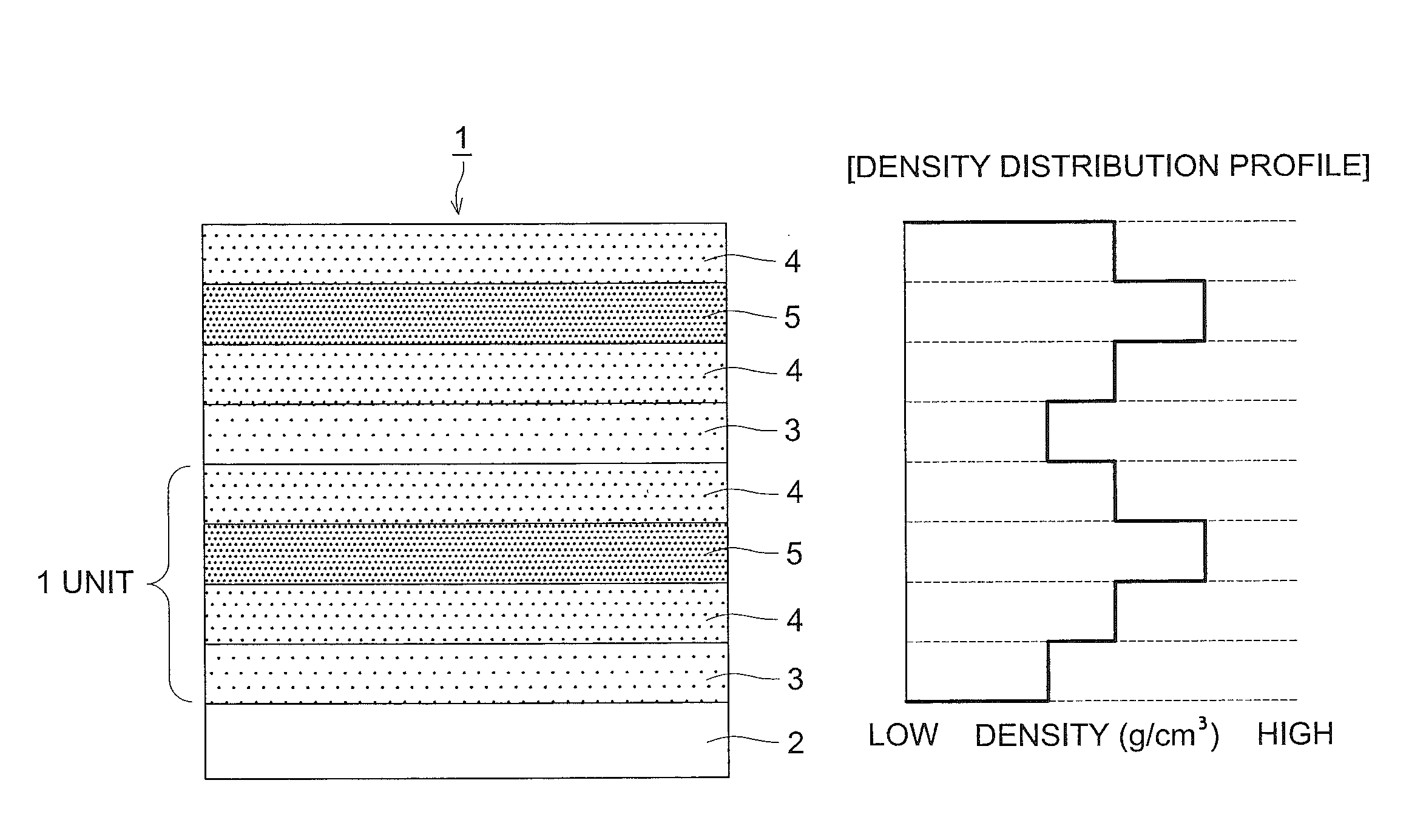
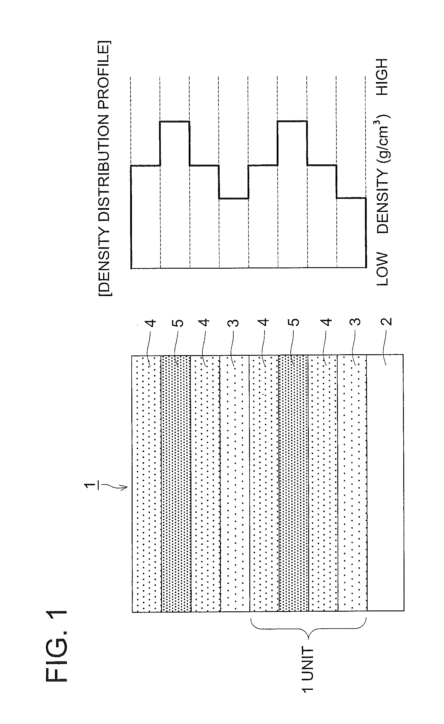
[0179]A transparent gas barrier film was prepared in such a manner that three units, each of which is composed of a low density layer, a medium density layer, a high density layer, and another medium density layer in that order are applied, onto a 100 μm thick polyethylene terephthalate film (produced by Teijin DuPont Ltd., and hereinafter referred to as PEN) under the following discharge conditions employing the following atmospheric pressure plasma discharge treatment apparatus to result in the density distribution profile shown in FIG. 1.

(Atmospheric Plasma Discharge Treatment Apparatus)

[0180]By employing the atmospheric plasma discharge treatment apparatus described in FIG. 2, a roller electrode covered with dielectric compounds and a set of plurality of square cylindrical electrodes were prepared as follows.

[0181]The roller electrode employed as the first electrode was prepared as follows. Titanium alloy T64 jacket roller metallic bas...

example 2

>

[0210]Under the same conditions as those which were employed to prepare Organic EL Element OLED1-1 described in Example 1, Organic EL Elements OLED5-1-3 were prepared, which were composed of materials and resulted in the film thickness described in Table 2 below. Further, under the same conditions as those which were employed to prepare Organic EL Element OLED2-1, Organic EL Elements OLED5-4-6, were prepared which were composed of materials and resulted in the film thickness, described in Table 2 below. Still further, under the same conditions as those which were employed to prepare Organic EL Element OLED3-1, Comparative Organic EL element OLED5-7 was prepared, which was composed of materials and resulted in the film thickness, described in Table 2 below.

TABLE 2Positive HoleElectronTransporting LayerTransporting(50 nm)Light Emitting Layer (50 nm)Layer (50 nm)CathodeOrganicRepeat-Repeat-Repeat-(100 nm)ELCon-ingHostDopantingCon-ingCon-Re-ElementstituentUnitMaterial(5 mol %)Unitstitu...

example 3

[0214]Organic EL Element 5-2 prepared in Example 2, a green light emitting organic EL element which was prepared in the same manner as Organic EL Element OLED5-2 of the present invention prepared in Example 2, except that the phosphorescent compound was replaced with Exemplified Compound Ir-1, and a red light emitting organic El element which was prepared in the same manner as Organic EL Element OLED5-2 of the present invention, except that the phosphorescent compound was replaced with Exemplified Compound Ir-9, were arranged on the same substrate, whereby the active matrix system full-color display device was prepared. In FIG. 5, only shown is the schematic view of display section A of the prepared full-color display device. Namely, on the same substrate, provided are a wiring section incorporating a plurality of scanning lines 205 and data lines 206, and a plurality of pixels 203 (such as pixels which emit light in the red, green or blue region). Scanning lines 205 and a plurality...


PUM

PropertyMeasurementUnit
acceleration voltageaaaaaaaaaa
fluorescentaaaaaaaaaa
fluorescence wavelengthaaaaaaaaaa

Abstract

In an organic electroluminescence element which incorporates a substrate having thereon an anode and a cathode and which incorporates a plurality of organic layers between the aforesaid anode and cathode, wherein at least one of the aforesaid organic layers is a first organic layer incorporating a compound having at most 10 repeating units, the first organic layer being prepared by coating the compound having at least one polymerizable group, followed by polymerization.

Description

CROSS REFERENCE TO RELATED APPLICATION[0001]The present application is a continuation application of U.S. patent application Ser. No. 11 / 817,271, filed on Aug. 28, 2007, the entire contents of which are incorporated herein by reference and priority to which is hereby claimed. The Ser. No. 11 / 817,271 is a U.S. national stage of application No. PCT / JP2006 / 302327, filed on 10 Feb. 2006, the entire contents of which are incorporated herein by reference and priority to which is hereby claimed. Priority under 35 U.S.C. §119(a) and 35 U.S.C. §365(b) is hereby claimed from Japanese Application No. 2005-057051, filed 2 Mar. 2005, the disclosure of which is also incorporated herein by reference.TECHNICAL FIELD[0002]The present invention relates to an organic electroluminescence element, a display device employing the same, and a lighting device.BACKGROUND[0003]Heretofore, cited as a light emitting type electronic display device has been an electroluminescence display (ELD). Constituting eleme...

Claims


Application Information

Patent Timeline
Patent Type & Authority Applications(United States)
IPC IPC(8): H01L51/54
CPCC09K11/06H05B33/14C09K2211/1044C09K2211/1059C09K2211/1092C09K2211/186C09K2211/188H01L51/004H01L51/0059H01L51/0062H01L51/0077H01L51/0081H01L51/0084H01L51/0085H01L51/0094H01L51/5012C09K2211/1029Y10S428/917H10K85/141H10K85/631H10K85/649H10K85/30H10K85/324H10K85/341H10K85/342H10K85/40H10K50/11H05B33/10
Inventor SUGITA, SHUICHIKITA, HIROSHITAKA, HIDEO
Owner MERCK PATENT GMBH
Why Eureka
Try Eureka