Semiconductor device and method for producing the same

a technology of semiconductors and transistors, applied in the direction of semiconductor devices, basic electric elements, electrical equipment, etc., to achieve the effects of low resistance, high on-breakdown voltage, and high off-breakdown voltag

Active Publication Date: 2011-05-05
SHARP KK
View PDF5 Cites 26 Cited by
  • Summary
  • Abstract
  • Description
  • Claims
  • Application Information

AI Technical Summary

Benefits of technology

[0077]According to the above production methods, the mutual relationship among the off-breakdown voltage, the on-breakdown voltage, and the on resistance can be improved, so that the semiconductor device can realize the low on resistance, the high off-breakdown voltage, and the high on-breakdown voltage.
[0078]According to the semiconductor device in the present invention, the mutual trade-off rela...

Problems solved by technology

However, when a higher breakdown voltage is realized in the LDMOS trans...

Method used


Image

  • Semiconductor device and method for producing the same
  • Semiconductor device and method for producing the same
  • Semiconductor device and method for producing the same

Examples


first embodiment

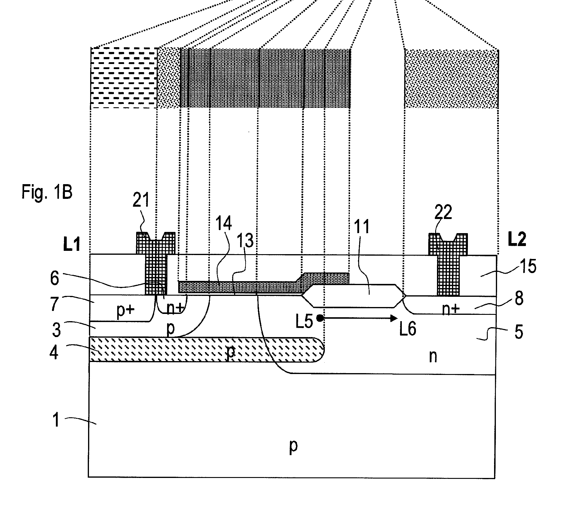
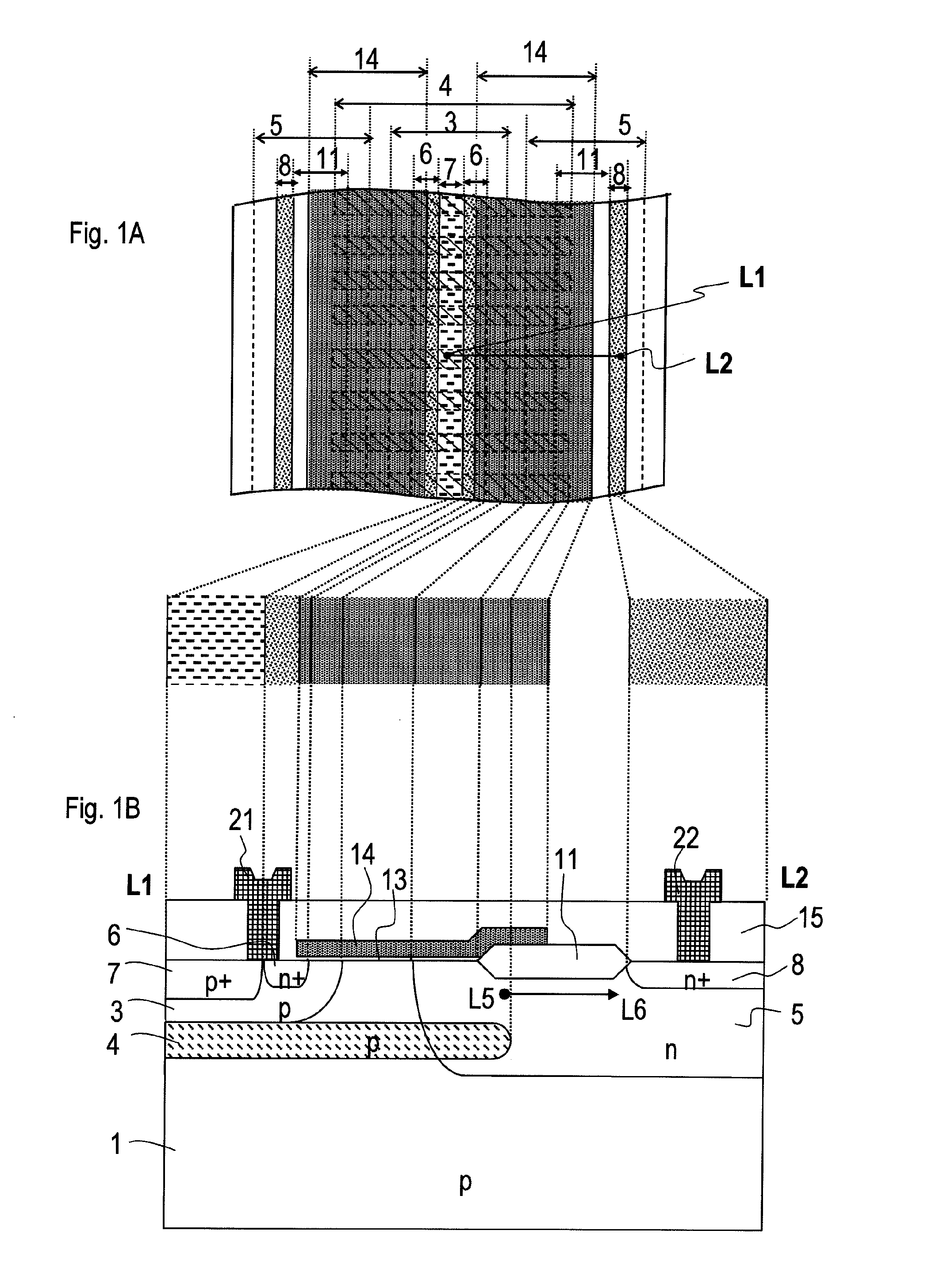
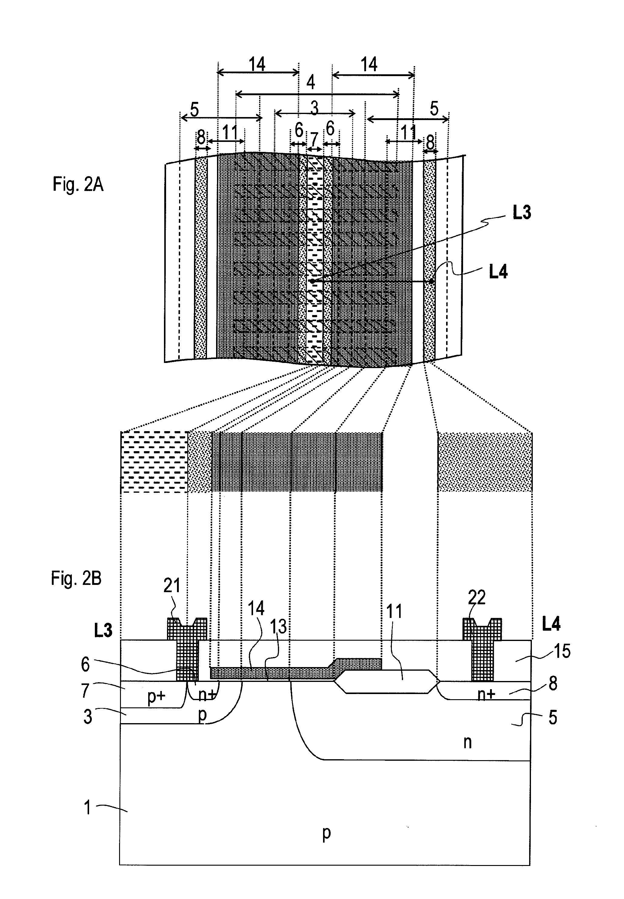
[0100]A description will be made of a first embodiment of a semiconductor device according to the present invention with reference to FIGS. 1A to 9C. In addition, the same component as that in FIG. 17 has the same reference in the following drawings and its description is omitted.

[0101]FIGS. 1A to 2B are schematic structure diagrams of an N channel LDMOS transistor serving as the semiconductor device in this embodiment. FIG. 1A and FIG. 2A are top schematic views, and both are totally the same. Meanwhile, FIG. 1B and FIG. 2B are both cross-sectional schematic views, but they are different in cut position such that FIG. 1B shows a cross-section cut along a line L1-L2, and FIG. 2B shows a cross-section cut along a line L3-L4.

[0102]In addition, these drawings are just shown schematically, so that an actual dimension ratio does not always coincide with a dimension ratio in the drawing. This is applied to the following drawings.

[0103]The N channel LDMOS transistor in this embodiment has ...

second embodiment

[0142]A description will be made of a second embodiment of a semiconductor device according to the present invention, with reference to FIGS. 10A to 12. In addition, the same component as that in FIGS. 17A and 17B or in the first embodiment has the same reference in each of the following drawings and its description is omitted.

[0143]A LDMOS transistor in this embodiment is the same as that of the first embodiment in that the P type embedded diffusion region 4 is discretely connected to the partial bottom surface of the P type body region 3, and each discrete part extends toward the drift region 5 such that its tip end reaches the inside of the drift region 5 to form the strip-shape. Meanwhile, it is different from that of the first embodiment in that an N type diffusion region 2 is provided on the P type semiconductor substrate 1, and the P type body region 3 and the N type drift region 5 are formed on this N type diffusion region 2. Hereinafter, the N type diffusion region 2 is ref...


PUM


Abstract

A P type semiconductor substrate includes a P type body region, an N type drift region formed away from the P type body region in a direction parallel to a substrate surface, an N type drain region formed in a region separated by a field oxide film in the N type drift region so as to have a concentration higher than the N type drift region, an N type source region formed in the P type body region so as to have a concentration higher than the N type drift region. A P type buried diffusion region having a concentration higher than the N type drift region is formed of a plurality of parts each of which is connected to a part of the bottom surface of the P type body region and extends parallel to the substrate surface and its tip end reaches the inside of the drift region.

Description

CROSS REFERENCE TO RELATED APPLICATION[0001]This Nonprovisional application claims priority under 35 U.S.C. §119(a) on Patent Application No. 2009-254439 filed in Japan on Nov. 5, 2009 the entire contents of which are hereby incorporated by reference.BACKGROUND OF THE INVENTION[0002]1. Field of the Invention[0003]The present invention relates to a semiconductor device and a method for producing the same and more particularly, to a LDMOS transistor (lateral double diffusion MOS transistor) and a method for producing the same.[0004]2. Description of the Related Art[0005]The LDMOS transistor has features of being high in switching speed, and being easily used because of an voltage drive system, and it is used for a switching regulator, various kinds of drivers, a DC-DC converter, and the like, taking advantage of the features, so that it becomes a key device in a present power-high breakdown voltage field.[0006]In general, a performance of the LDMOS transistor is represented by a break...

Claims


Application Information

Patent Timeline
IPC IPC(8): H01L29/78H01L21/336
CPCH01L29/063H01L29/0634H01L29/0692H01L29/0696H01L29/1045H01L29/7835H01L29/1095H01L29/42368H01L29/66659H01L29/66681H01L29/7816H01L29/1083
Inventor ICHIJO, HISAOADAN, ALBERTO
Owner SHARP KK
Why Eureka
Try Eureka