Package structure and manufacturing method thereof
a technology of packaging and manufacturing method, applied in the direction of semiconductor devices, semiconductor/solid-state device details, electrical devices, etc., can solve the problems of reducing the distance of the signal transmission path, affecting the operability, performance and life of the ic chip, and the traditional package technique cannot meet the demand of producing a smaller chip with high density elements on the chip, etc., to achieve the effect of reducing the thickness of the package structur
- Summary
- Abstract
- Description
- Claims
- Application Information
AI Technical Summary
Benefits of technology
Problems solved by technology
Method used
Image

Examples
first embodiment
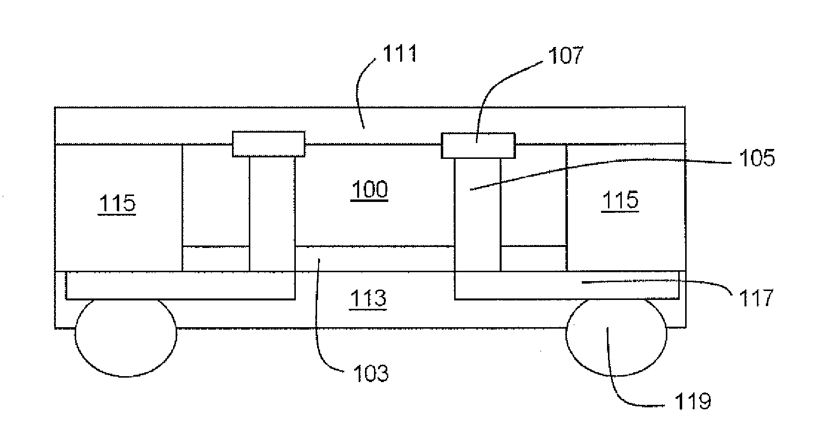
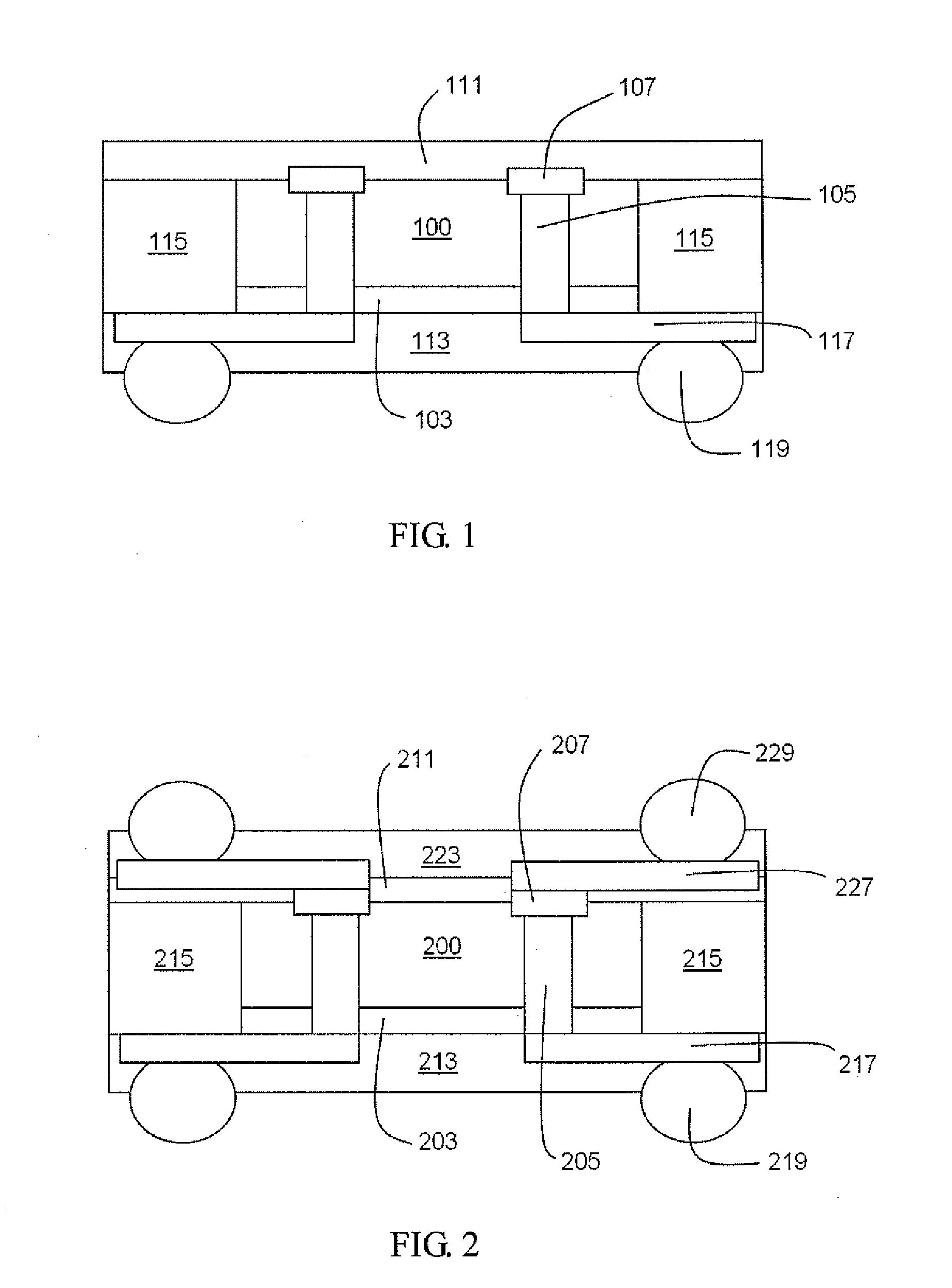
[0029]FIG. 1 illustrates a cross-sectional view of a semiconductor device package structure according to the present invention. As shown in FIG. 1, a semiconductor device package structure includes an electronic element 100, which comprises an active surface and a backside surface, and includes a dielectric (isolation) layer 103 formed on the backside surface of the electronic element 100. A plurality of conductive through vias 105 cross through the electronic element 100 and the dielectric layer 103, and a plurality of conductive pads 107 accompany the conductive through vias 105 disposed on the active surface of the electronic element 100. A filler 115 is adjacent to the side wall of the electronic element 100 and the side wall of the dielectric layer 103. A redistribution layer 117 is formed under the dielectric layer 103 and connects to the conductive through vias 105. A first protective layer 111 is formed to cover and protect the active surface of electronic element 100, the c...
second embodiment
[0034]FIG. 2 illustrates a cross-section view of a stacked semiconductor device package structure according to the present invention. As shown in FIG. 2, a stacked semiconductor device package structure includes electronic element 200, which comprises an active surface and a backside surface and includes a dielectric (isolation) layer 203 formed on the backside surface of the electronic element 200. A plurality of conductive through vias 205 cross through the electronic element 200 and the dielectric layer 203, and a plurality of conductive pads 207 accompany the conductive through vias 205 disposed on the active surface of the electronic element 200. A filler 215 is adjacent to the side wall of the electronic element 200 and the side wall of the dielectric layer 203. A first redistribution layer 217 is formed under the dielectric layer 203 and connects to the conductive through vias 205. A first protective layer 211 is formed to cover and protect the active surface of electronic el...
third embodiment
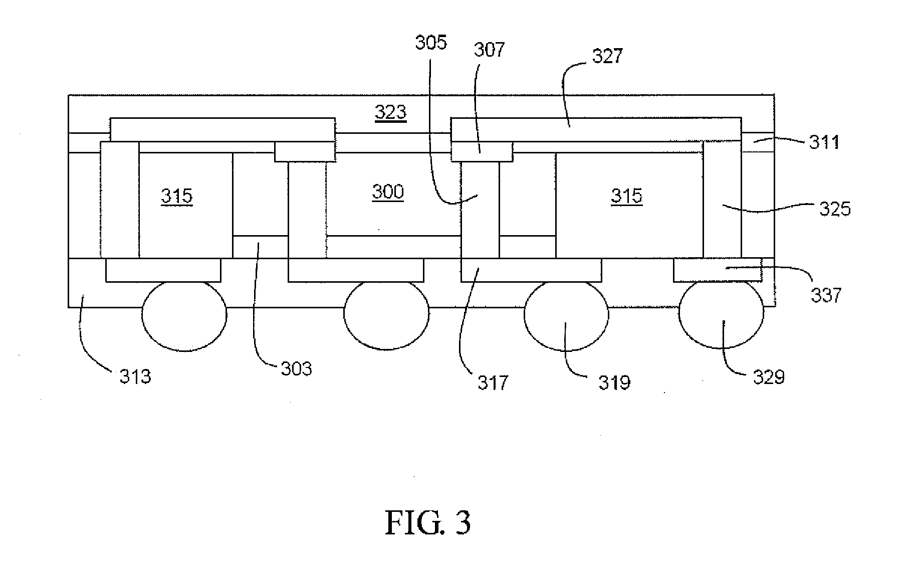
[0039]FIG. 3 illustrates a cross-section view of a semiconductor device package structure according to the present invention. As shown in FIG. 3, a semiconductor device package structure includes an electronic element 300, which comprises an active surface and a backside surface and includes a dielectric (isolation) layer 303 formed on the backside surface of the electronic element 300. A plurality of first conductive through vias 305 cross through the electronic element 300 and the dielectric layer 303, and a plurality of conductive pads 307 accompany the first conductive through vias 305 disposed on the active surface of the electronic element 300. A filler 315 is adjacent to the side wall of the electronic element 300 and the side wall of the dielectric layer 303. A first redistribution layer 317 is formed under the dielectric layer 303 and connects to the conductive through vias 305. A plurality of second conductive through vias 325 further formed across through the filler 315. ...
PUM
 Abstract
Description
Claims
Application Information
 - R&D
- Intellectual Property
- Life Sciences
- Materials
- Tech Scout
- Unparalleled Data Quality
- Higher Quality Content
- 60% Fewer Hallucinations
Browse by: Latest US Patents, China's latest patents, Technical Efficacy Thesaurus, Application Domain, Technology Topic, Popular Technical Reports.
© 2025 PatSnap. All rights reserved.Legal|Privacy policy|Modern Slavery Act Transparency Statement|Sitemap|About US| Contact US: help@patsnap.com