This helps you quickly interpret patents by identifying the three key elements:
Problems solved by technology
Method used
Benefits of technology
Benefits of technology
[0011]An advantage of some aspects of the invention is to provide an atomic oscillator having a relatively simple structure by improving the degree of freedom of design.
[0015]Accordingly, according to the aspect of the invention, as compared with the related art atomic oscillator, the degree of freedom of design is improved, and the atomic oscillator having the relatively simple structure can be provided.
Problems solved by technology
However, in the related art atomic oscillator, the oscillator, such as the PLL, to generate the modulation frequency fm1, which accurately coincides with the frequency of ½ of the frequency (for example, 9.19263 . . . GHz in the case of a cesium atom) corresponding to ΔE12, directly or by harmonics must be prepared specially, and the degree of freedom of design is restricted.
Method used
Image
Click on the blue label to locate the original text in one second.
Reading with bidirectional positioning of images and text.
Examples
first embodiment
(1) First Embodiment
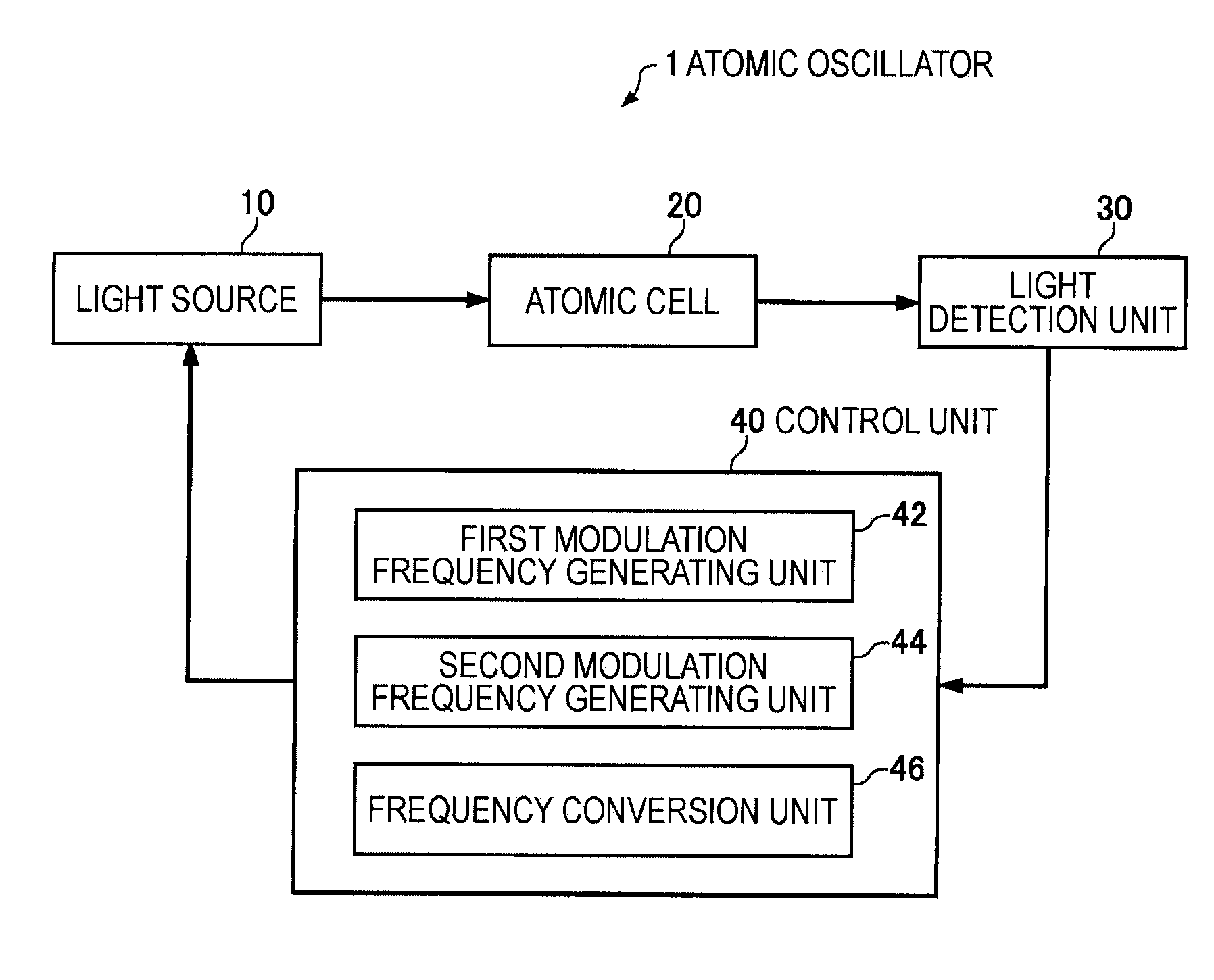
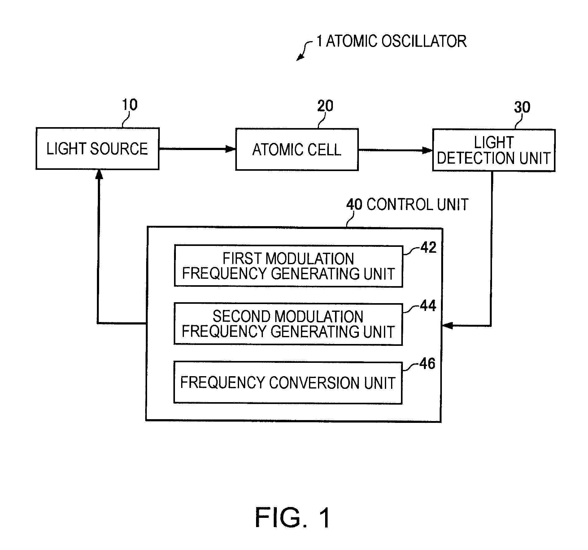
[0058]FIG. 5 is a view showing a structure of an atomic oscillator of a first embodiment.
[0059]As shown in FIG. 5, the atomic oscillator 100A of the first embodiment includes a semiconductorlaser 110, an atomic cell 120, a light detector 130, a detector circuit 140, a low frequency oscillator 150, a current drive circuit 160, a detector circuit 170, a low frequency oscillator 180, a detection modulation circuit 190, a first modulation frequency generating circuit 200 and a second modulation frequency generating circuit 210.
[0060]The atomic cell 120 is such that gaseous alkali metal atoms (natrium (Na) atoms, rubidium (Rb) atoms, cesium (Cs) atoms, etc.) are sealed in a container.
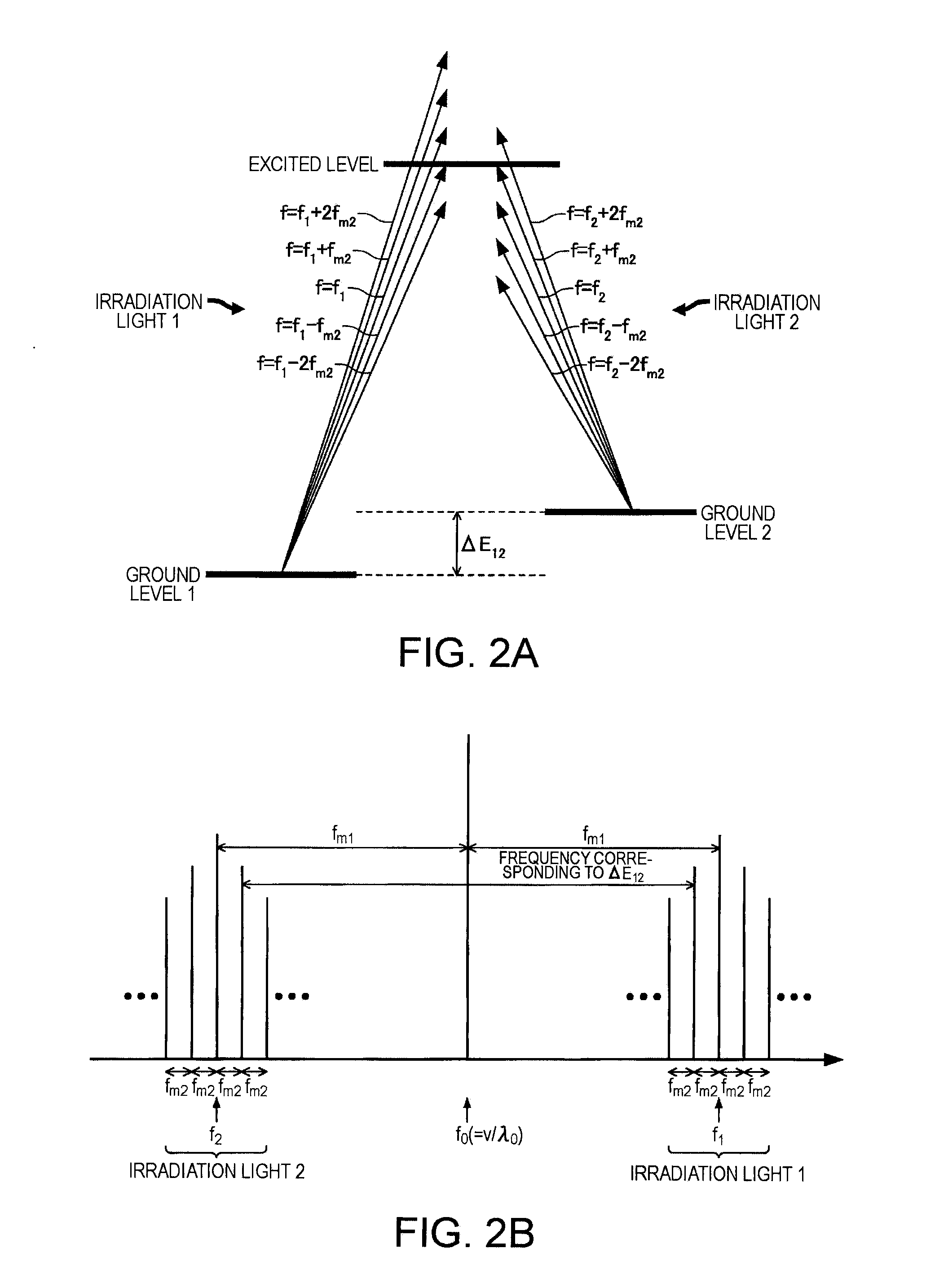
[0061]When a pair of resonant lights having a frequency difference coincident with a frequency corresponding to an energy difference between two ground levels of the alkali metal atom are simultaneously irradiated to the atomic cell 120, the alkali metal atom causes the EIT phenomenon. F...
modified example
[0089]FIG. 8 is a view showing a structure of a modified example of the atomic oscillator of the first embodiment. As shown in FIG. 8, in an atomic oscillator 100B of the modified example, an electro-optic modulator (EOM) 220 is added to the atomic oscillator 100A shown in FIG. 5.
[0090]As shown in FIG. 8, in the atomic oscillator 100B, a semiconductorlaser 110 is not modulated by a first modulation signal having a first modulation frequency fm1 or a second modulation signal having a second modulation frequency fm2, and emits a laser light having a frequency f0 to the electro-optic modulator (EOM) 220.
[0091]The first modulation signal modulated by a detection modulation circuit 190, together with the second modulation signal, is inputted to the electro-optic modulator (EOM) 220.
[0092]The electro-optic modulator (EOM) 220 modulates the laser light having the frequency f0 by the first modulation signal and the second modulation signal. As a result, in the light passing through the ele...
second embodiment
(2) Second Embodiment
[0096]FIG. 9 is a view showing a structure of an atomic oscillator of a second embodiment. As shown in FIG. 9, in the atomic oscillator 100C of the second embodiment, a connection relation between a first modulation frequency generating circuit 300 and a second modulation frequency generating circuit 310 is opposite to the connection relation between the first modulation frequency generating circuit 200 and the second modulation frequency generating circuit 210 in the atomic oscillator 100A of the first embodiment shown in FIG. 5.
[0097]In the atomic oscillator 100C, the second modulation frequency generating circuit 310 generates a second modulation signal having a second modulation frequency fm2 corresponding to a voltage of an output signal of a detector circuit 170.
[0098]The second modulation signal is modulated by an oscillation signal (equal to an oscillation signal supplied to the detector circuit 170) of a low frequency oscillator 180, and is supplied to ...
PUM
Abstract
An atomic oscillator using an electromagnetically induced transparency phenomenon caused by irradiation of a resonant light pair to an alkali metal atom, includes: a light source that generates a first light having a center frequency f1 and a plurality of frequency components different from each other in frequency by Δf, and a second light having a center frequency f2 and a plurality of frequency components different from each other in frequency by Δf; a light detection unit that detects intensities of lights including the first light and the second light passing through the alkali metal atom; and a control unit that controls, based on a detection result of the light detection unit, to cause a frequency difference between a specified frequency component of the first light and a specified frequency component of the second light to be equal to a frequency corresponding to an energy difference between two ground levels of the alkali metal atom, wherein a frequency difference between the center frequency f1 of the first light and the center frequency f2 of the second light is different from the frequency corresponding to the energy difference between the two ground levels of the alkali metal atom.
Description
[0001]The entire disclosure of Japanese Patent Application No. 2009-258872, filed Nov. 12, 2009 is expressly incorporated by reference herein.BACKGROUND[0002]1. Technical Field[0003]The present invention relates to an atomic oscillator.[0004]2. Related Art[0005]An atomic oscillator based on an electromagnetically induced transparency (EIT) system (also called a coherent populationtrapping (CPT) system) is an oscillator using a phenomenon in which when two resonant lights different from each other in wavelength (frequency) are simultaneously irradiated to an alkali metal atom, the absorption of the two resonant lights is stopped.[0006]It is known that the interaction mechanism between the alkali metal atom and the two resonant lights can be explained in a Λ-type three-level system model as shown in FIG. 13A. The alkali metal atom has two ground levels, and when resonant light 1 having a wavelength (frequency f1) corresponding to an energy difference between the ground level 1 and th...
Claims
Application Information
Patent Timeline
Application Date:The date an application was filed.
Publication Date:The date a patent or application was officially published.
First Publication Date:The earliest publication date of a patent with the same application number.
Issue Date:Publication date of the patent grant document.
PCT Entry Date:The Entry date of PCT National Phase.
Estimated Expiry Date:The statutory expiry date of a patent right according to the Patent Law, and it is the longest term of protection that the patent right can achieve without the termination of the patent right due to other reasons(Term extension factor has been taken into account ).
Invalid Date:Actual expiry date is based on effective date or publication date of legal transaction data of invalid patent.

