Carbon nanotube film structure and method for manufacturing the same

a carbon nanotube and film structure technology, applied in the field of carbon nanotube film structure, can solve the problems of disposing a cnt, unable to apply a well-known integrated circuit production process that requires coating of resists or the like, and it is difficult to manufacture high density aligned cnt film structures, etc., to achieve the effect of facilitating design, high density cnt, and further integration

Inactive Publication Date: 2011-05-12
NAT INST OF ADVANCED IND SCI & TECH
View PDF3 Cites 24 Cited by
  • Summary
  • Abstract
  • Description
  • Claims
  • Application Information

AI Technical Summary

Benefits of technology

[0016]The present invention has been accomplished in view of the situations in the prior art and it mainly intends to provide a CNT film structure of high quality in which a CNT layer having a plurality of CNTs aligned continuously in one identical direction along a film plane and having high density and uniform thickness is deposited above a substrate, that is, a CNT film structure having a CNT film of an optional shape having excellent physical property and a substrate of an optional shape and material.
[0061]Further, according to the invention, a high density CNT thin film in which a plurality of CNTs are aligned in one direction within a film plane can be provided easily. Since the CNT thin film has the same physical property as described above and the well-known pattering technique and etching technique are applicable thereto, compatibility with the integrated circuit production process is enhanced and the thin film can be used suitably to the manufacture of wafers for forming electronic devices, MEMS devices or electronic circuits.

Problems solved by technology

That is, in the prior art, it was extremely difficult to dispose a CNT layer of optional shape to an optional position of an optional substrate and production of high density aligned CNT film structure was substantially impossible.
Further, since a CNT film formed by a CVD method or the like generally had a low weight density in a state as formed, it was impossible to apply a well-known integrated circuit production process that requires coating of a resist or the like.
Further, for a CNT aggregate in which the alignment degree of CNTs is low or CNTs are not aligned at all, a gap between individual CNTs in the assembly is inevitably increased and the filling density is not increased sufficiently even when they are compressed, for example, by applying an external pressure (refer to FIG. 2(a)) and integrity and solidness capable of satisfying desired mechanical property cannot be obtained.
The problems described above result significant impediments in using a CNT film structure to an application use, for example, of MEMS that requires mechanical operation.

Method used


Image

  • Carbon nanotube film structure and method for manufacturing the same
  • Carbon nanotube film structure and method for manufacturing the same
  • Carbon nanotube film structure and method for manufacturing the same

Examples


example 1

Demonstration Example 1

[0315]Result of demonstrating the controllability for the film thickness and the weight density before and after the densifying treatment in the densifying step of the invention is shown below. As the experimental conditions for this purpose, for obtaining a desired number of CNT films of a desired thickness, the width of the metal catalyst film served for the chemical vapor deposition step (thickness of the CNT film before densification) was defined as 1 μM for 2 sets, 2 μm for 1 set, 4 μm for 2 sets, and 7.5 μm for 4 sets.

[0316]The result is to be described with reference to FIG. 18. As shown in FIG. 18(a), while the CNT film having a thickness before densification (original thickness) of 7.5 μm shrank to about 0.5 μm in average after densification, CNT films having original thickness of 1, 2, 4 μm, shrank to 0.2 μm to 0.3 μm respectively after densification. This suggests that the density is different after densification depending on the original thickness....

example 2

Demonstration Example 2

[0322]The degree of anisotropy, that is, the degree of alignment property can be recognized by measuring the resistivity of a CNT thin film by a 4 terminal method. The 4-terminal method is carried out, for example, as shown in FIG. 20, by placing a CNT thin film 5 on a measuring site in which four Au electrodes 7a to 7d each of 2 μm width are arranged each at 2 μm distance.

[0323]The resistivity was measured by the 4-terminal method in this demonstration example, as shown in FIG. 21, by providing a measuring substrate equipped with 6-sets of the measuring sites shown in FIG. 20, and providing CNT thin films each having a thickness of 306 nm, a weight density of 0.28 g / cm3, and an average diameter of 2.8 nm, and CNT thin films each having a thickness of 835 nm, a weight density of 0.19 g / cm3, and an average diameter of 2.8 nm patterned with measuring portions of the lateral size (1, 2, 5, 10 μm for parallel direction, 2.5 μm for perpendicular direction) differen...

example 3

Demonstration Example 3

[0326]For the CNT thin film having a thickness of 450 nm, a weight density of CNT of 0.46 g / cm3, and an average diameter of CNT of 2.8 nm, alignment property was evaluated quantitatively by the Herman's orientation factor.

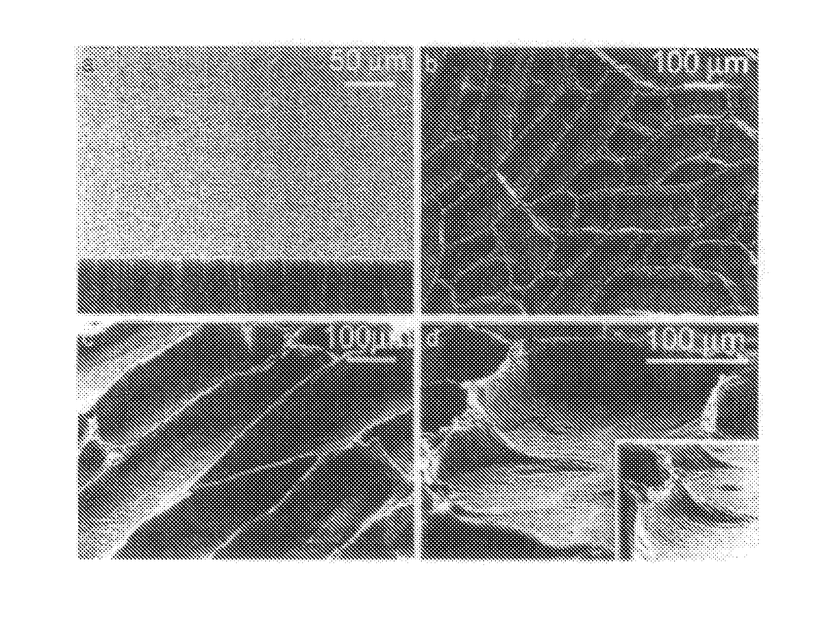
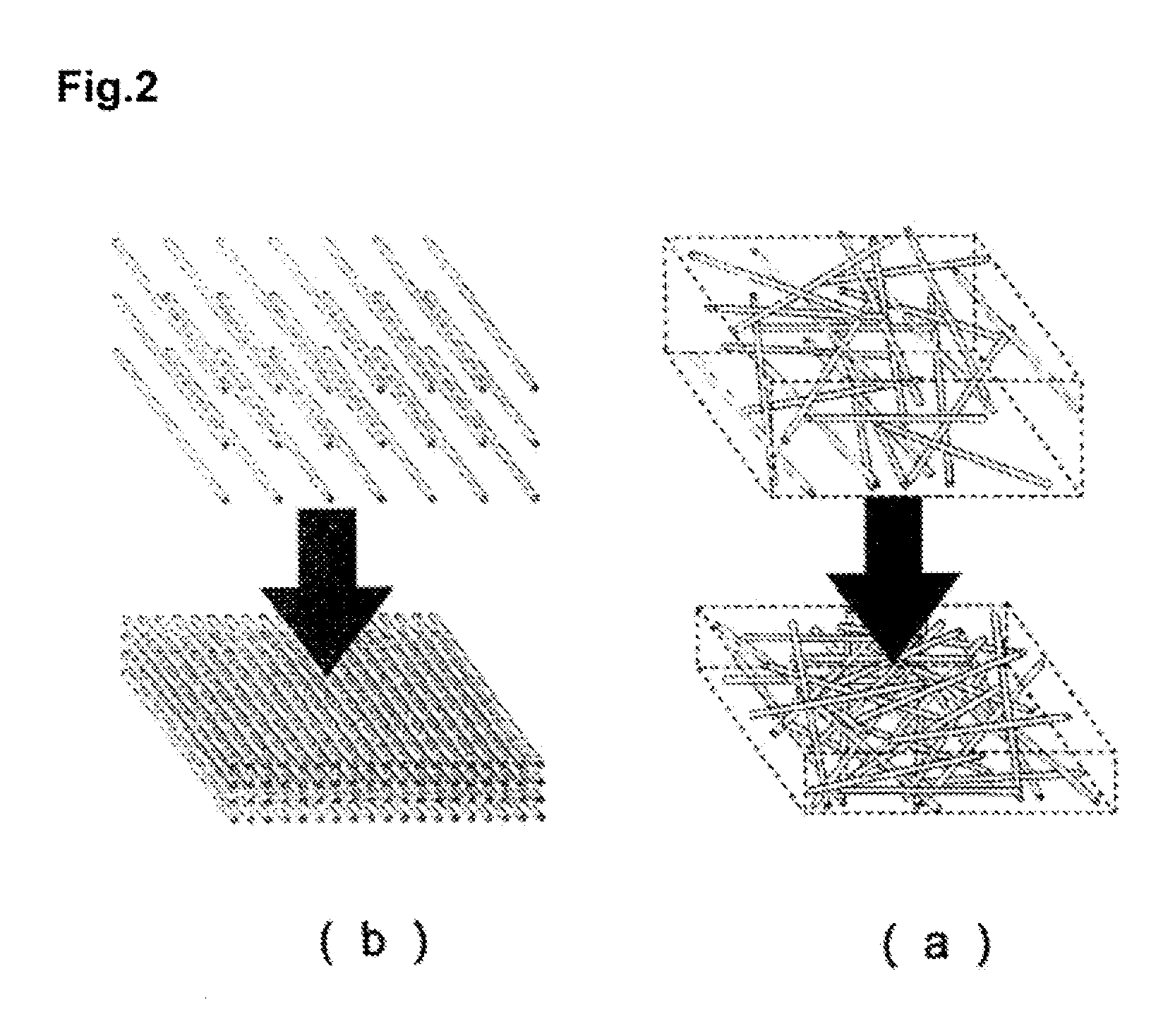
[0327]FIG. 23 shows an atomic force microscope (AFM) image processed so as to exhibit the degree of unevenness on the surface of a CNT thin film adhered to the planar substrate and FIG. 24 shows a planar image representing the distribution of unevenness in each direction by a frequency distribution by Fast Fourier Transformation (FFT) of the AFM image.

[0328]It has been recognized already in FIG. 23 that CNTs extend in the vertical direction and, in FIG. 24 representing the same by a frequency distribution for each of the directions, the profile for the frequency distribution forms a flat elliptic shape with the abscissa being as a major axis. This represents that CNTs are aligned in the vertical direction in FIG. 23. Then, as the ellipsis bec...


PUM

PropertyMeasurementUnit
weight densityaaaaaaaaaa
densityaaaaaaaaaa
thicknessaaaaaaaaaa

Abstract

A method of producing a carbon nanotube film structure having a substrate and a carbon nanotube layer, comprises a placing step of placing a carbon nanotube film comprising a plurality of carbon nanotubes aligned in one direction within a film plane on the substrate; and a densifying step of applying a densifying treatment to the carbon nanotube film thereby forming the carbon nanotube layer having the weight density of the carbon nanotube to 0.1 g / cm3 or more. Thus, a problem of island-like shrinkage caused while a highly densified CNT layer is being manufactured is solved, and a high-quality CNT film structure wherein the aligned CNT layer having a high density and uniform thickness is deposited on the substrate.

Description

FIELD OF THE INVENTION[0001]The present invention relates to a carbon nanotube film structure, and a production process thereof. More specifically the invention also relates to a carbon nanotube film structure in which a carbon nanotube layer formed by aligning a plurality of carbon nanotubes continuously in one direction within a film plane is deposited on a substrate, and a production process thereof. Further, the invention also relates to a carbon nanotube thin film in which a plurality of carbon nanotubes are aligned in one direction within a film plane, and a production process thereof.BACKGROUND ART[0002]A momentum has been increased for applying carbon nanotube (hereinafter also referred to as CNT) as a constituent material for Micro Electro Mechanical Systems (MEMS) devices or electronic devices in the field of nanotechnology. For obtaining such devices, it has been demanded for a CNT film structure in which a CNT layer including a film-like CNT aggregate comprising a plural...

Claims


Application Information

Patent Timeline
Patent Type & Authority Applications(United States)
IPC IPC(8): B32B3/00B32B38/00B05D3/02B32B38/16B32B5/02B29C39/00C01B31/02B82Y40/00
CPCB81B2203/0127B81C1/0038B82Y30/00B82Y40/00C01B31/022C01B2202/08Y10T428/24612Y10T428/30Y10T156/1041Y10T428/24479Y10T428/24851Y10T156/1028Y10T428/24521C01B2202/10Y10T428/249924
Inventor HATA, KENJIHAYAMIZU, YUUHEIYAMADA, TAKEO
Owner NAT INST OF ADVANCED IND SCI & TECH
Why Eureka
Try Eureka