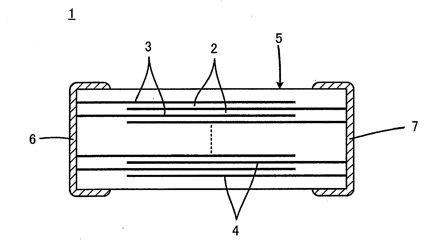
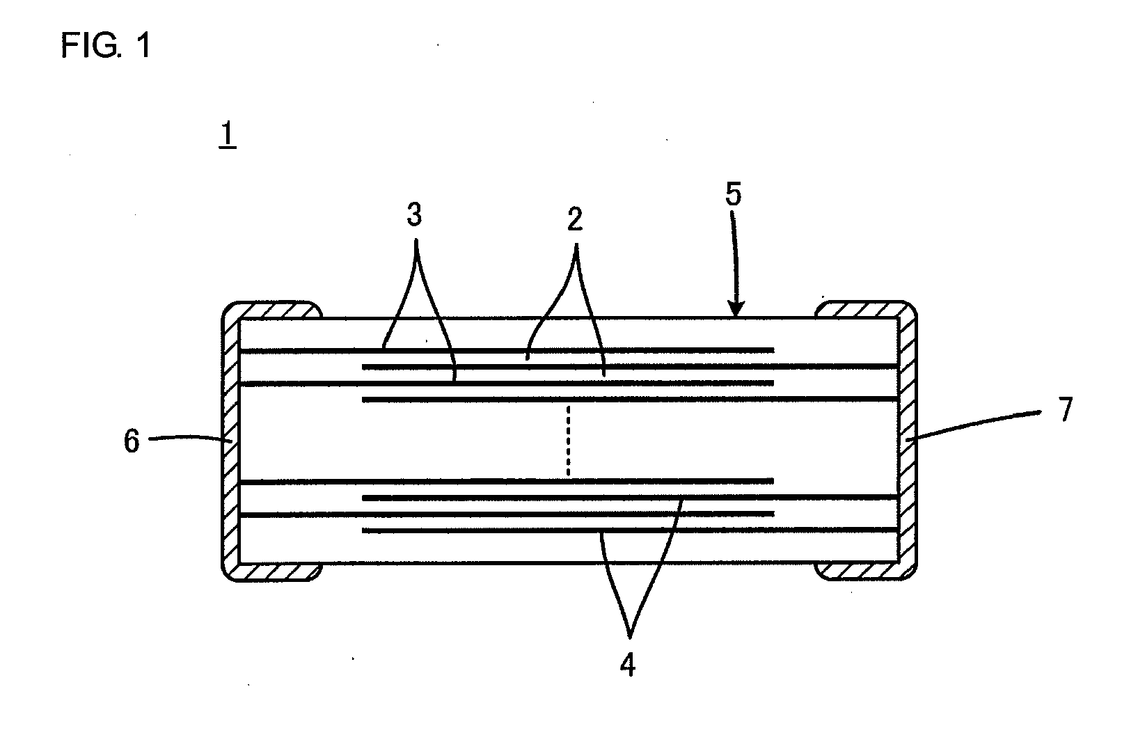
Dielectric ceramic and laminated ceramic capacitor
a technology of laminated ceramic and dielectric ceramic, which is applied in the direction of stacked capacitors, fixed capacitor details, fixed capacitors, etc., can solve the problems of reducing the defect of withstand voltage, and the decrease of the dielectric constant of the dielectric ceramic, so as to reduce the residual stress, reduce the insulation resistance, and reduce the effect of residual stress
- Summary
- Abstract
- Description
- Claims
- Application Information
AI Technical Summary
Benefits of technology
Problems solved by technology
Method used
Image
Examples
experimental example 1
[0053]For the purpose of producing a main constituent powder, respective powders of BaCO3, CaCO3, and TiO2 were prepared, and each weighed in predetermined amounts, and then, after the addition of pure water and a dispersant, a further grinding and crushing treatment was carried out with the use of a forced-circulation wet grinding mill (using PSZ media). The treated slurry was dried in an oven, and then subjected to a heat treatment at a temperature of 950° C. or more, thereby providing a (Ba, Ca)TiO3 based main constituent powder with an average grain size of 0.15 to 0.25 μm.
[0054]Subsequently, for the purpose of producing a dielectric raw material powder, respective powders of Re2O3, MgCO3, MnCO3, V2O5, and SiO2 were prepared in addition to the main constituent powder, and each weighed in predetermined amounts, and then, after the addition of pure water and a dispersant, a further grinding and crushing treatment was carried out with the use of a forced-circulation wet grinding mi...
experimental example 2
[0091]In Experimental Example 2, samples were produced in the same way as in the case of Experimental Example 1, but the ratio e / b of the SiO2 content to the MgO content was varied while the Ca content x, the type of Re and the Re content a, the Mg content b, the Mn content c, the V content d, and the Si content e fell within the scope of the present invention, as shown in Table 3.
TABLE 3Sam-CaReMgMnVSipleCon-Con-Con-Con-Con-Con-Num-tentRetenttenttenttenttentberxTypeabcdee / b610.05Gd / Dy0.1 / 0.70.50.50.052.55.0620.05Gd / Dy0.1 / 0.70.50.50.0524.0630.05Gd / Dy0.1 / 0.70.50.50.051.53.0640.05Gd / Dy0.1 / 0.71.50.50.0521.3650.05Gd / Dy0.1 / 0.71.50.50.051.51.0660.05Gd / Dy0.1 / 0.71.50.50.050.750.5670.05Gd / Dy0.1 / 0.70.150.50.05320.0680.05Gd / Dy0.1 / 0.70.170.50.052.514.7690.05Gd / Dy0.1 / 0.70.20.50.051.68.0700.05Gd / Dy0.1 / 0.71.50.50.050.50.3710.05Gd / Dy0.1 / 0.71.50.50.050.020.01
[0092]In Table 3, the ratio e / b falls within the range of 0.5 to 5.0 for samples 61 to 66, whereas the ratio e / b falls outside the range of 0.5...
PUM
| Property | Measurement | Unit |
|---|---|---|
| dielectric constant | aaaaa | aaaaa |
| grain size | aaaaa | aaaaa |
| temperature | aaaaa | aaaaa |
Abstract
Description
Claims
Application Information

